Samsung will launch 1.4nm technology, BSPDN back power supply, and silicon photon technology in 2027
Samsung's wafer foundry department recently revealed that it is expected to launch 1.4nm process technology, chip back power supply network (BSPDN), and silicon photonics technology in 2027. Samsung held a Samsung OEM forum in San Jose, USA on June 13th, revealing some of the company's roadmap in the era of artificial intelligence (AI).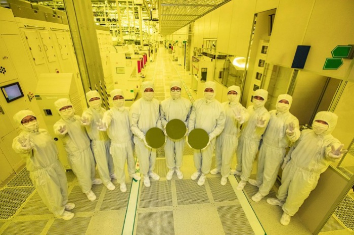
Siyoung Choi, the head of Samsung's wafer foundry business unit, emphasized in his keynote speech that high-performance and low-power chips are the most important factors in achieving AI. The company has also launched a turnkey one-stop service called "Samsung Artificial Intelligence Solutions", which allows customers to leverage Samsung's wafer foundry, storage chip, and advanced packaging services. Samsung stated that this will simplify the customer's supply chain and increase its product release speed by 20%. The company revealed that its AI related orders have surged by 80% in the past year.
During this forum, Samsung also shared its plan to launch silicon photonics technology in 2027, marking the first time Samsung has announced the adoption of silicon photonics technology. This technology utilizes optical fiber to transmit data on chips, which can significantly improve I/O data transmission speed compared to traditional cables/circuits. In addition, Samsung has also invested in Celestial AI, a silicon photonic technology company.
Samsung stated that the 2nm process using BSPDN technology will also be launched in 2027. This is later than its competitor Intel's plan to launch similar technologies in 2024. BSPDN technology designs power supply circuits on the back of the wafer to avoid signal lines and prevent mutual interference. This technology can significantly improve chip power, performance, and area efficiency.
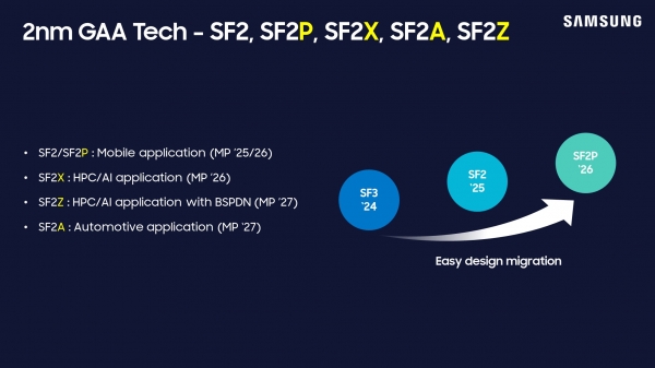
Samsung has revealed its 2nm process roadmap: SF2 and SF2P for mobile applications will be launched in 2025 and 2026, respectively; The 2nm process for artificial intelligence and high-performance computing (HPC) will be launched in 2026, ahead of the BSPDN process. The company will also launch a 2nm process for automobiles in 2027.
Samsung reiterated its plan to launch the 1.4nm process in 2027 and is currently ensuring the performance and yield of the technology. The company plans to adopt ASML High NA EUV lithography machines for 1.4nm process chip manufacturing by 2025.
Samsung reiterated its plan to launch the 1.4nm process in 2027 and is currently ensuring the performance and yield of the technology. The company plans to adopt ASML High NA EUV lithography machines for 1.4nm process chip manufacturing by 2025.