Samsung accelerates the development of glass substrates and strives for mass production by 2026
Previously, it was reported that Samsung has formed a new cross departmental alliance, spanning electronics, electrical engineering, and display departments, to collaborate and accelerate the commercial research and development of "glass substrate" technology, with the hope of achieving mass production in 2026. Samsung aims to achieve commercialization faster than Intel, and in the past, its subsidiary Samsung Electric was mainly responsible for promoting the project.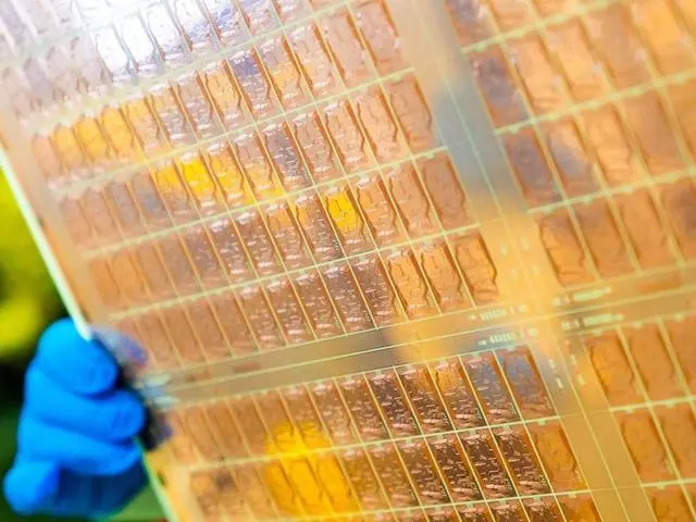
According to ETNews, Samsung is accelerating the development of semiconductor glass substrate technology, advancing procurement and installation to September, and starting trial operations in the fourth quarter of this year, a full quarter ahead of the initial plan. Samsung hopes to start producing glass substrates for high-end system level packaging (SiP) in 2026, and in order to secure orders in 2026, it needs to be ready by 2025 to demonstrate sufficient capabilities.
Samsung plans to make all necessary preparations for installing equipment on the trial production line before September. The selection of suppliers has been completed, including Philoptics, Chemtronics, Joongwoo M-Tech, and LPKF from Germany, which will provide the corresponding components. There are reports that Samsung's setup is aimed at simplifying production and strictly adhering to its safety and automation standards.
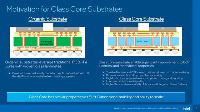
Compared with traditional organic substrates, glass substrates overcome the drawbacks of traditional methods and have significant advantages, including excellent flatness, improved lithography focus, and outstanding dimensional stability in next-generation system level packaging with multiple small chip interconnections. In addition, glass substrates have better thermal and mechanical stability, making them more suitable for high-temperature and durable application environments required by data centers.
Samsung plans to make all necessary preparations for installing equipment on the trial production line before September. The selection of suppliers has been completed, including Philoptics, Chemtronics, Joongwoo M-Tech, and LPKF from Germany, which will provide the corresponding components. There are reports that Samsung's setup is aimed at simplifying production and strictly adhering to its safety and automation standards.
Compared with traditional organic substrates, glass substrates overcome the drawbacks of traditional methods and have significant advantages, including excellent flatness, improved lithography focus, and outstanding dimensional stability in next-generation system level packaging with multiple small chip interconnections. In addition, glass substrates have better thermal and mechanical stability, making them more suitable for high-temperature and durable application environments required by data centers.
Last September, Intel expressed its hope to become the industry leader in the production of next-generation advanced packaging glass substrates. Its internal team has spent nearly a decade on research and development, and plans to conduct trial production at a production base in Arizona, with plans to use it for commercial products by 2030.
Samsung wafer foundry is currently trying to secure more orders for data center products and also needs to provide more advanced packaging services to assist. These efforts on glass substrates may have a crucial impact on the future.
Samsung wafer foundry is currently trying to secure more orders for data center products and also needs to provide more advanced packaging services to assist. These efforts on glass substrates may have a crucial impact on the future.