Restore growth! The global semiconductor packaging materials market is expected to reach $26 billion next year
Recently, SEMI, TECHCET, and TechSearch International announced in their latest Global Semiconductor Packaging Materials Outlook (GSPMO) report that the global semiconductor packaging materials market is expected to begin a growth cycle driven by strong demand for semiconductors from various end applications, with a projected compound annual growth rate (CAGR) of 5.6% until 2028. The report emphasizes that although this niche market is still emerging and currently has low unit production, artificial intelligence remains an expected growth driver for advanced packaging applications.The GSPMO report provides comprehensive data and predictions on substrates, lead frames, bonding wires, and other advanced packaging materials.
TECHCET President and CEO Lita Shon Roy said, "The semiconductor packaging materials market experienced a 15.5% decline in 2023, and our latest report predicts that growth will resume in 2024. It is expected that by 2025, the global packaging materials market will exceed $26 billion and continue to steadily grow until 2028
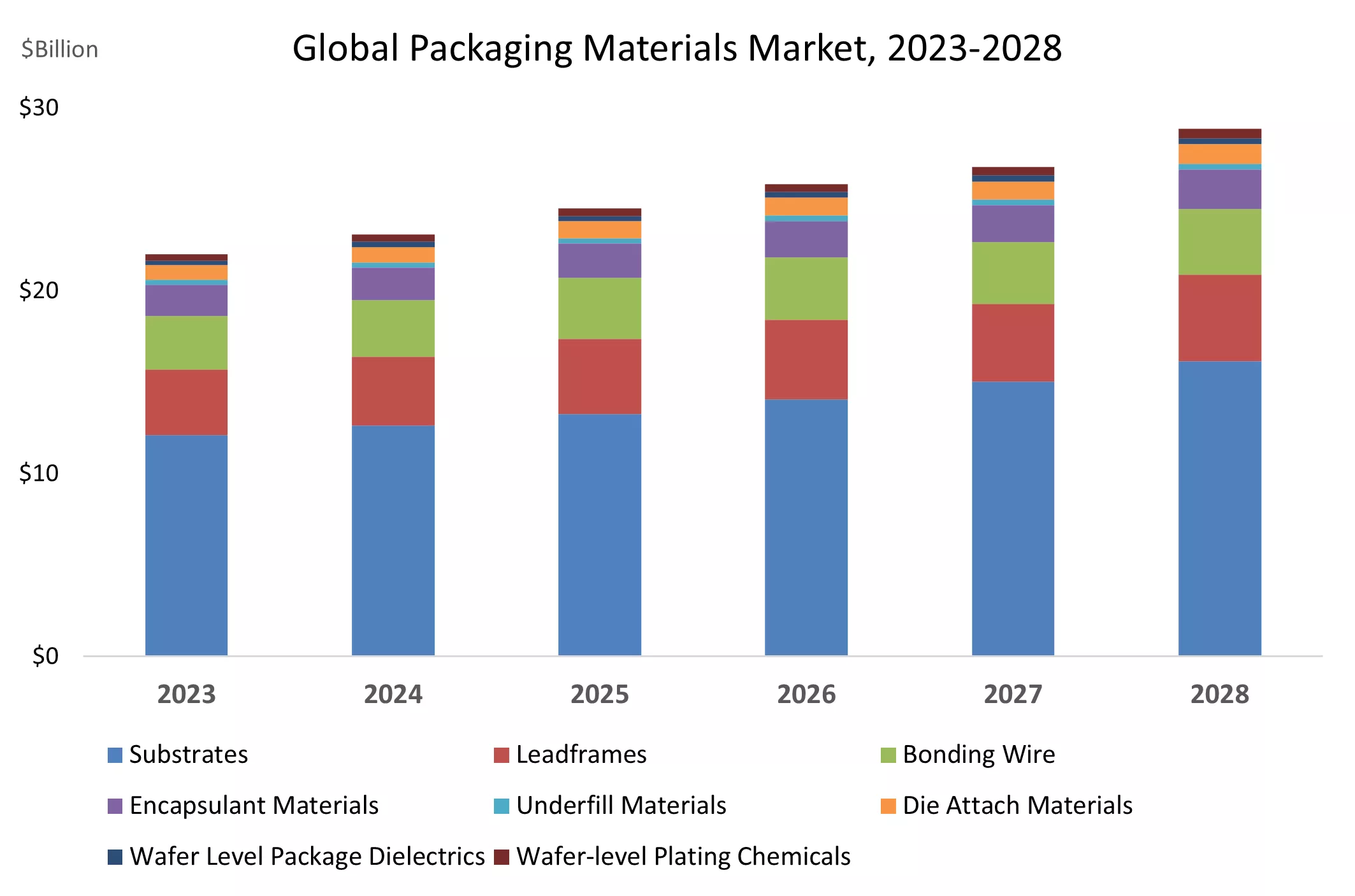
TechSearch International President Jan Vardaman said, "PCBs account for a significant portion of the packaging materials market revenue, and in this category, FC-BGA substrates account for the majority of revenue growth From 2023 to 2028, the compound annual growth rate of revenue from flip chip BGA/LGA is expected to be 7.6%. Other key growth areas include wafer level packaging (WLP) dielectrics and flip chip bottom filling. Annual sales in the laminated substrate segment are expected to increase by 7.3%, while lead frames and bonding wires are also expected to recover, growing by 5.0% and 6.4%, respectively