News reports that Intel has increased orders for advanced packaging equipment and materials
Industry insiders have revealed that Intel has increased its orders to multiple equipment and material suppliers to develop the next generation of advanced packaging based on glass substrate technology, expected to enter mass production by 2030.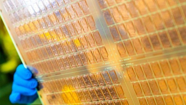
Advanced packaging will play an important role in extending Moore's Law, as it has the potential to increase transistor density and unleash the powerful computing power of high-performance computing.
Sources say that Intel sees advanced packaging as a strategy to defeat TSMC in the field of contract manufacturing, and the company also competes with TSMC in advanced 3nm and below process production.
Intel has invested approximately $1 billion in the past decade to establish a glass substrate research and development line and supply chain at its Arizona factory, with an expected launch of a complete glass substrate solution from 2026 to 2030.
According to Intel, glass substrates have excellent mechanical, physical, and optical properties, allowing for the connection of more transistors in packaging, resulting in greater scalability and larger system level packaging than organic substrates. The company plans to launch a complete glass substrate solution to the market in the second half of this decade, enabling the industry to push Moore's Law beyond 2030.
The glass substrate has received attention and investment from multiple enterprises. Samsung Electromechanical, a subsidiary of Samsung Group, announced in March the establishment of a joint research and development (R&D) united front with major electronic subsidiaries such as Samsung Electronics and Samsung Display to develop glass substrates. The company will begin large-scale production in 2026, aiming to achieve commercialization faster than Intel, which entered glass substrate research and development a decade ago. And Apple is actively participating in PCBs made from glass substrates.