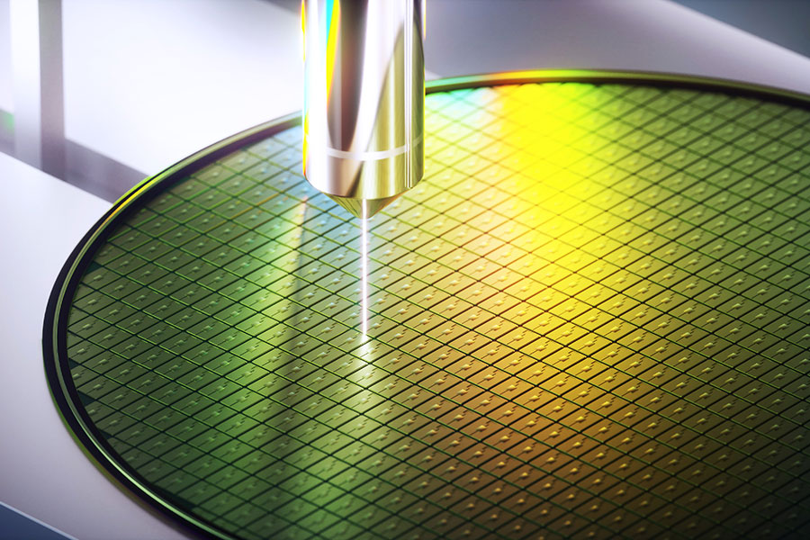
Japan restarts 0.5-inch small wafer fab to cultivate semiconductor talents
Talent cultivation is a key challenge for Japan to revitalize its semiconductor industry. For this reason, the Japanese government has chosen to restart the 0.5-inch wafer technology, which was previously used as a teaching and introductory tool.
Ceatec 2024, Japan's largest digital technology exhibition, will highlight their efforts by showcasing existing equipment and conditions.
After TSMC announced the Kumamoto plant project, the Japanese government and academic institutions launched a wide-ranging initiative to investigate and build infrastructure to revitalize Japan's semiconductor industry. However, the survey results show that more than half of Japanese young students still do not understand the career opportunities in the semiconductor manufacturing industry, nor do they know which educational programs can guide them into the industry. Therefore, Japan's policy goals include establishing a semiconductor talent training system and promoting semiconductor education programs.
According to reports, the construction cost of each advanced semiconductor wafer fab is estimated to be around 2 trillion yen (13.1 billion US dollars). Due to the need to invest a large amount of funds and time, it is difficult to meet the demand for teaching and demonstration venues, thus requiring low-cost semiconductor production lines for educational use.
Japan launched a low-cost semiconductor manufacturing program called Small Wafer Factory in 2012. This plan provides customized 0.5-inch wafer manufacturing equipment for small and medium-sized enterprises. This technology was created to achieve mass production of memory chips, and this market is mainly occupied by manufacturers in South Korea and Taiwan, China, China, using 8 inch and 12 inch production lines.
The current advantage of small wafer fabs is that the construction cost of the entire production line is about 500 million yen, which is only 1/4000 of the cost of traditional wafer fabs. Due to the limited surface area of 0.5-inch wafers, there is no need for a dedicated clean room for heat treatment and vacuum treatment during the production process. The vacuum heating box is very small and can be placed on a desk. It is powered by a regular 100V/110V power supply and does not require industrial electricity.
In theory, a complete small-scale wafer fab technology semiconductor production line can be established in a regular high school physics and chemistry laboratory. Although the output power of this production line is very small and largely inconspicuous, it is still sufficient to meet the teaching objectives.