Japan has developed a new technology for heating flat wafer substrates, which is superior to traditional grinding and polishing methods
According to a report on the Nikkei Chinese website, a research team led by Professor Seimatsu Hang of Waseda University in Japan has developed a method to flatten the surface of semiconductor wafer substrates by heating, which is more convenient and high-performance than traditional grinding methods, and is beneficial for improving semiconductor manufacturing processes.
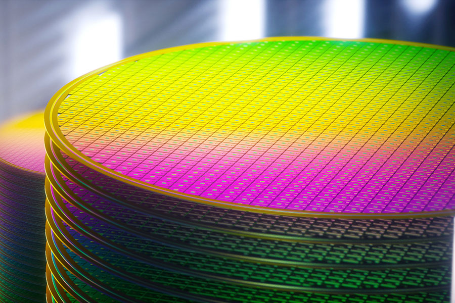
The research team conducted experiments using silicon carbide wafer substrates. Due to the fact that wafers are manufactured by cutting the entire crystal block into thin slices, the cross-section is prone to unevenness and cannot be directly used. The traditional method is to combine multiple methods for polishing and grinding, but this can lead to internal damage and surface drop formation.
The team will heat the mechanically ground silicon carbide substrate under argon and hydrogen protection for 10 minutes to 1600 degrees Celsius, and then maintain it at 1400 degrees Celsius for a period of time. At this point, the surface reaches an atomic level of flatness. Due to its simple operation method, which only requires heating, compared to traditional multiple polishing, it is beneficial to shorten manufacturing hours and reduce costs.
In addition to processing power semiconductor material silicon carbide, this technology can also be used to process other materials with similar lattice structures, such as gallium nitride and gallium arsenide wafers.