Canon: Nanoimprinting technology is expected to manufacture 2nm semiconductors
Canon Corporation of Japan announced on October 13th the launch of FPA-1200NZ2C nanoimprint (NIL) semiconductor manufacturing equipment. Canon CEO Fujio Mitarai has stated that the company's new nanoimprinting technology will pave the way for small semiconductor manufacturers to produce advanced chips, and this technology is currently almost entirely owned by the largest companies in the industry.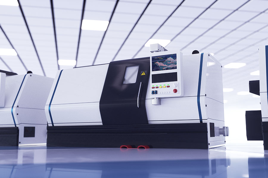
When explaining nanoimprinting technology, Iwamoto Kazunori, the head of Canon's semiconductor equipment business, stated that nanoimprinting technology involves imprinting a mask with a semiconductor circuit diagram onto a wafer. By only imprinting once on a wafer, complex two-dimensional or three-dimensional circuits can be formed in the appropriate position. If the mask is improved, even products with a circuit linewidth of 2nm can be produced. Currently, Canon's NIL technology enables the minimum linewidth of the pattern to correspond to a 5nm node logic semiconductor.
It is reported that the 5nm chip manufacturing equipment industry is dominated by ASML, and Canon's nanoimprinting method may help narrow the gap.
In terms of equipment costs, Iwamoto and Takashi stated that customer costs vary depending on the conditions, and it is estimated that the cost required for one lithography process can sometimes be reduced to half of traditional lithography equipment. The reduction in scale of nanoimprinting equipment also facilitates the introduction of applications such as research and development. Canon CEO Fujio Mitarai has stated that the price of the company's nanoimprinting equipment products will be one digit lower than ASML's EUV (Extreme Ultraviolet) equipment, but the final pricing decision has not been made yet.
It is reported that Canon has received many inquiries from semiconductor manufacturers, universities, and research institutes regarding its customers. As an alternative product to EUV equipment, nanoimprinting equipment is highly anticipated. This device can be used for various semiconductor applications such as flash memory, personal computer DRAM, and logic.