Understanding the D Latches in Digital Systems
In digital electronics, improving circuit parts is needed for better system stability and function. One big step is moving from SR latches to D latches. D latches make inputs simpler and cut down on undefined states, making them better in designing and reliable in digital memory systems. This article looks at the D latch's design, how it works, and its uses, highlighting its importance in modern circuits. We will cover its basic structure, how it works, and how it fits into complex systems with multiplexers. By examining these aspects, we understand how the D latch improves data integrity and predictability in digital systems, enhancing the efficiency and reliability of electronic components.Catalog
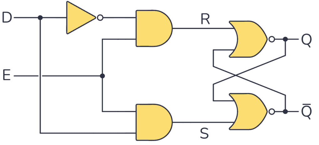
Figure 1: The D Latch
The D Latch Circuits
The development of electronic latch circuits has seen many important changes, leading to the creation of the D latch, a better version of the gated S-R latch. At first, the gated S-R latch used set (S) and reset (R) inputs, managed by an enable signal to control when the latch would operate. However, these early designs had problems with undefined states, which could cause the system to fail. By removing the reset input and using the opposite of the set input as the only control method, the input process became much simpler, making the system more predictable and easier to use. This change ensured that the outputs, Q and not-Q, were always opposites, making the operation more stable and reliable.
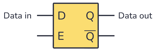
Figure 2: D Latch Symbol
The D Latch Structure
The main feature of the D latch is its single-input system, which replaces the two-input design of the older S-R latch. This single input, called the Data input (D), simplifies the latch's operation.
In the D latch, the output is controlled by two signals: the Data input (D) and the Enable signal (E). When the Enable signal is active, the Data input (D) determines the state of the output (Q). If the Data input is 1, the output (Q) will also be 1. If the Data input is 0, the output (Q) will be 0. The other output, not-Q, is always the opposite of Q. This means that if Q is 1, not-Q will be 0, and vice versa.
This relationship between Q and not-Q ensures that the outputs are always predictable and stable. The D latch's structure eliminates the issues found in the older S-R latch, where having two inputs could sometimes lead to undefined states. These undefined states could cause the circuit to malfunction.
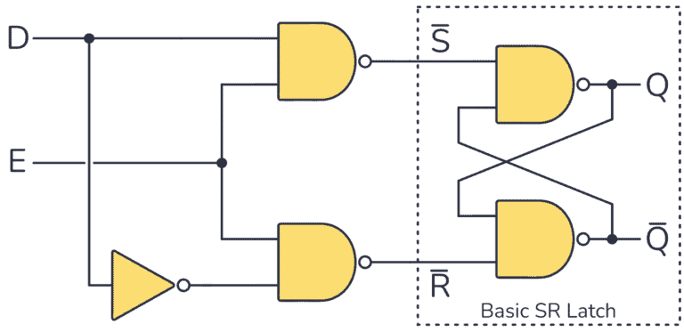
Figure 3: D Latch Circuit
Standardized D Latches in Electronics
The D latch is not simply a theoretical idea. It's a real, integral part found in a lot of electronics. You can find it as a pre-packaged circuit component, which means it’s ready-made and easy to use in any projects. In electronic schematics, the D latch is shown by a standard symbol, making it easy to recognize and understand. This standardized symbol is important because it shows how widely used the D latch in the electronics industry.
The D latch acts as a basic memory unit in any types of computing systems. It helps store and keep track of binary data, best for proper functioning of these systems. Because the D latch is standardized, it ensures that its functionality is consistent in electronic applications.
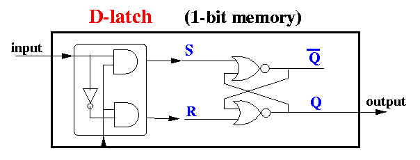
Figure 4: D Latch In Memory Storage
Role of D Latch in Digital Memory Systems
It works by allowing data to be inputted when an enable signal is high. When this signal is high, whatever data comes in gets captured and held by the D latch. As soon as the enable signal drops to low, the D latch stops accepting new data and maintains the last piece of data it received. And it keeps the data stable and unchanged, even if there are changes in the incoming data after the enable signal has been turned off. This characteristic of the D latch is extremely important for the storage of memory. It means that once data is stored, it remains safe and unaltered, which is good for data integrity, especially in systems where data needs to be reliable and constant over time. The ability of the D latch to hold onto a single bit of data reliably under various conditions makes it a main player in memory storage systems. It is particularly effective in environments where data should be retained accurately. The D latch is highly adaptable, making it valuable in digital applications. In programmable logic controllers, it can replace traditional S-R latches in ladder logic diagrams, demonstrating its flexibility across electronic and computing environments. This versatility ensures the D latch remains relevant in a rapidly evolving technology.
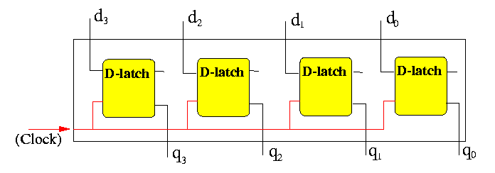
Figure 5: 4 Bit Memory Constructed Using Four D-Latches
Design and Circuit Analysis of the D Latch
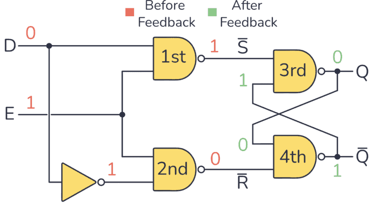
Figure 6: D Latch Circuit and Logic Gates
The D latch marks a positive advancement in digital circuit design by addressing the limitations of the SR latch. It overcomes the issue of indeterminate states caused when both Set (S) and Reset (R) inputs are high in an SR latch. This improvement is achieved by simplifying the input scheme to a single data input, known as D, and introducing an inverter to ensure the inputs are always complementary.
This design offers some advantages. Primarily, it guarantees predictable state transitions based on the value of the D input. When D is low, the latch's next state is set to zero; when D is high, the next state is set to one. This predictability directly mirrors the SR latch's truth table but with enhanced reliability. The D latch maintains data integrity as long as the enable condition is met, making it good in digital circuits, particularly in applications requiring dependable data storage such as memory devices and register elements.
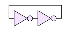
Figure 7: Back-To-Back Inverter of D Latch
Constructing a D latch using basic digital components like NAND gates and inverters provides a tangible understanding of its operation and benefits. This hands-on approach is especially useful in educational settings, allowing students and enthusiasts to observe and analyze the latch's behavior under various enable conditions. Through practical experiments, learners gain deeper insights into digital memory storage and signal control. Observing how the D latch responds to many inputs and maintains its state reinforces the importance of circuit design in achieving reliable digital functionality. This experimentation highlights the need for complementary inputs to avoid indeterminate states, solidifying the learner's grasp of digital latch design principles.
The D latch circuit enhances the SR latch by adding logic gates to prevent invalid states and improve functionality. An inverter on the D input, combined with NAND gates, introduces an Enable (E) input that controls when data is captured. This setup ensures that the latch only captures data from the D input to the Q output when the enable signal is active, providing precise control for data buffering and timing applications. The circuit's adaptability is further demonstrated through potential configurations using many gate types, such as AND and NOR gates, showcasing its versatility in digital logic scenarios.
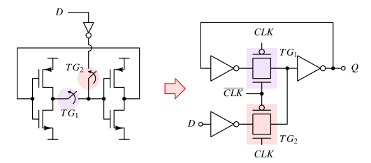
Figure 8: Modifying The Back-to-Back Inverter Based Latch To A Usable D-Latch
D Latch's Truth Table
Understanding the operational guidelines of the D latch is require for its application in digital circuits. The D latch's truth table provides a clear overview of how the latch responds to input and clock signal combinations. This truth table is an appropriate tool for designers, allowing them to predict the latch's behavior under different conditions and ensure the circuit functions correctly within its intended applications.
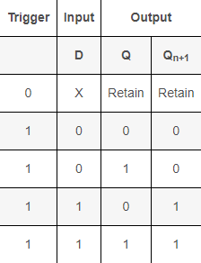
Figure 9: D Latch's Truth Table
Circuit Analysis of the D Latch
A detailed analysis of the D latch circuit shows a strategic arrangement of NAND gates that maintain signal integrity and prevent state conflicts. The pathway from input to output is carefully mapped, demonstrating how each component ensures the latch functions correctly under varying conditions. This breakdown is right for understanding how the D latch achieves consistent reliability, emphasizing the precision required in digital circuit design.
The D latch is a required memory component in digital circuits, capable of either preserving its current state or updating it based on the Enable input. This behavior is outlined in the D latch's truth table. When the Enable input is low, the latch ignores changes at the D input, maintaining its current state. When the Enable input is high, the Q output matches the D input. In digital memory systems and logic circuits, the D latch's capacity to hold or selectively update ensures data stability and predictable outputs. The timing dynamics of the D latch are best understood through its timing diagram, which shows how the input and output interact with the Enable signal. When the Enable is active, the output Q mirrors the input D. When the Enable is inactive, the latch retains its last state. It can be helpful to comprehend the D latch's behavior in relation to changes in the Enable signal, particularly through the use of this graphic representation. These insights are valuable for designing, troubleshooting, and optimizing circuits that incorporate the D latch. Exploring the D latch design through back-to-back inverters reveals alternative approaches that meet specific electronic design requirements and constraints. This method emphasizes the D latch's adaptability and innovative potential in digital memory storage solutions.
Multiplexer-Based D Latch Design
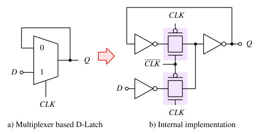
Figure 10: A Multiplexer Based D Latch
Further streamlining and customization of the D latch can be achieved by incorporating a multiplexer (MUX). A multiplexer selects between different data inputs based on a control signal, allowing the D latch to handle multiple data sources within the same circuit configuration. This capability is particularly useful in complex systems where multiple data inputs should be processed and stored conditionally. Integrating a multiplexer with a D latch enhances functionality by accommodating multiple input sources while maintaining the simplicity of the latch design. It is beneficial in applications requiring rapid switching between different data inputs under controlled timing conditions, such as in communication systems or complex computational units. Using a multiplexer to create a D latch highlights the flexibility of latch design, showing how standard digital components can be reconfigured to perform similar functions in many ways. This method enhances understanding of digital logic design principles and their practical applications, increasing versatility in circuit design.
Standard of Gated D Latches
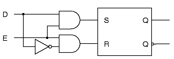
Figure 11: Gated D Latch Circuit
Logic Diagram of Gated D Latch
The logic diagram of a gated D latch is a key tool for building and analyzing these digital circuits. It shows how the circuit works in detail, which is good for designing or maintaining digital electronic systems. By showing every connection and component, the diagram helps understand how the D latch functions.
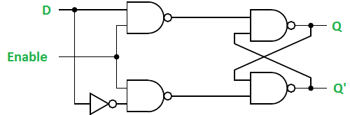
Figure 12: Logic Diagram of Gated D Latch
This diagram also shows improvements over the basic D latch. One major improvement is adding extra control mechanisms to better store and retrieve data. These changes make the gated D latch more reliable and efficient, enhancing its performance in digital electronics.
Improvements include features like enabling and disabling the latch based on control signals, which prevent unwanted data changes during difficult operations. This keeps data accurate throughout the circuit's operation, which is part in complex digital systems where precision is important. The logic diagram serves as a guide for building or fixing the gated D latch and helps in understanding digital circuits better.
Role of Gated D Latch in Digital Circuits
Adding gating to the D latch design improves control in digital circuits, making data storage more predictable and stable. The gated D latch allows for timed data control, aligning storage with specific operational phases in digital systems. This precision right for applications requiring exact timing and strict state management in advanced digital circuits. As a basic memory element, the D latch is needed for managing state changes and data within digital circuits. Maintaining data integrity and reliability requires precise timing and accurate data inputs. The D latch captures and holds data based on control signals, ensuring updates only happen at the right times, which prevents errors and data corruption.
Truth Table of Gated D Latch
The truth table for the gated D latch outlines specific outcomes based on input conditions. It serves as a definitive guide for predicting the latch's behavior in scenarios, enhancing the design and functionality of digital circuits that use this component.
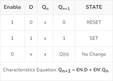
Figure 13: Truth Table of Gated D Latch
Conclusion
Knowing the D latch shows its part in boosting the performance on modern digital systems. Unlike older SR latches, the D latch brings predictability and stability, especially for today’s technology. Its simple input system prevents uncertain states and keeps data intact under different conditions. The use of multiplexers and gated versions shows the D latch's flexibility and ongoing development to meet advanced technology needs. Its standard use in any platforms confirms its importance in digital circuit design. This article has shown the technical benefits of the D latch and its greatly impact on digital memory system development, making it best tool for engineers and designers in digital electronics.
Frequently Asked Questions [FAQ]
1. What is the D latch?
The D latch (Data latch or Transparent latch) is a simple type of flip-flop circuit, primarily used for storing binary data. It consists of a data input, an output, and a control signal input, commonly referred to as the enable or clock input. The primary part of a D latch is to capture and hold a binary input value, making it available at the output as long as the control signal permits.
2. What is the function of the gated D latch?
The gated D latch functions as a data storage device that allows data to be stored and retrieved based on the state of its control signal. When the enable (or clock) input is active, the latch "listens" to the data input and passes it to the output. When the enable input is inactive, the output retains the last data value that was input while the enable signal was active.
3. Which gate is the D latch based on?
The D latch is typically based on NAND or NOR gates. These gates are configured in such a way that they create a feedback loop, allowing the device to maintain its output state (store data) even after the input condition changes.
4. How to make a D latch?
To construct a D latch, you start by arranging NAND or NOR gates into a feedback circuit. The basic setup involves using two gates to create a loop that maintains output until the control signal changes. Connect the data input to one of the gates whose output feeds into a second gate, which in turn controls the first gate's operation based on the enable signal condition.
5. What is the function of the D latch?
As noted, the function of the D latch is to store a single bit of data and provide a stable output as long as the control signal remains unchanged. It serves as a basic memory unit in electronic systems, capturing and holding data dynamically as required by the system.
6. Why is gated D latch called transparent latch?
The gated D latch is called a transparent latch because when the enable signal is active, changes at the data input are directly reflected at the output, then making the latch "transparent" to the passage of data. This transparency has real-time data processing where immediate updates to the output are needed.
7. How does D-latch store data?
A D-latch stores data using its feedback loop mechanism. When the enable signal is active, the data input is fed through the gates to set the output state. As soon as the enable goes inactive, the output of the gates is looped back to its inputs, maintaining the last state indefinitely until the enable is activated again with new data. This looping back of output to input is what allows the D-latch to hold data without external refresh.