TL494 Current-Mode PWM Controller IC
The TL494 is a flexible pulse-width modulation (PWM) controller used in automotive, industrial, and consumer electronics. This article explores its design, including pin layout, features, internal structure, and real-world applications. It also discusses how the TL494 improves system reliability and energy efficiency by looking at main parts like its dual error amplifiers, flexible output transistors, and built-in oscillator. Practical details, recommended settings, and circuit diagrams illustrate its usefulness for modern engineering needs.Catalog
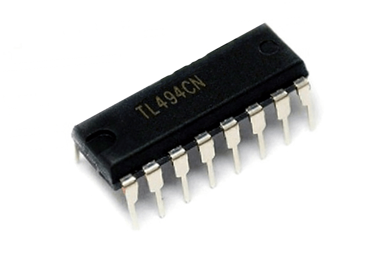
Figure 1: TL494 Series - TL494CN
What Is the TL494 PWM Controller?
The TL494 is an integrated circuit primarily used for managing power distribution in electronic devices through a process called pulse-width modulation (PWM). It’s designed to regulate power supplies efficiently across various systems. This chip provides all components required to build a PWM control system independently.
The chip contains several elements that ensure smooth power management. It includes two error amplifiers that help correct voltage fluctuations, and a tunable oscillator that adjusts the frequency of the PWM signal. Also, built-in circuits manage timing and regulate the output, allowing the TL494 to fine-tune power supply circuits based on specific performance needs.
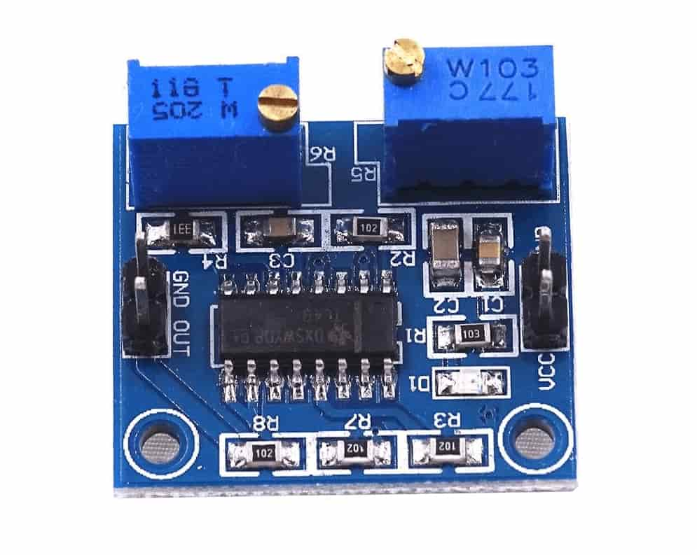
Figure 2: TL494 PWM Controller Module
The TL494 offers flexibility in how power is output. It can operate in both single-ended and push-pull configurations, ensuring stable and consistent power delivery. A built-in voltage regulator maintains a reliable 5-volt reference with 5% accuracy for steady performance.
TL494 Pinout Configuration
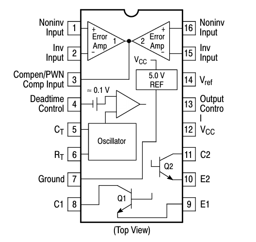
Figure 3: TL494 Pinout
|
Pin Name |
Pin No. |
Description |
|
1IN+ |
1 |
Noninverting input to error amplifier 1 |
|
1IN- |
2 |
Inverting input to error amplifier 1 |
|
FEEDBACK |
3 |
Input pin for feedback |
|
DTC |
4 |
Dead-time control comparator input |
|
CT |
5 |
Capacitor terminal used to set the oscillator frequency |
|
RT |
6 |
Resistor terminal used to set the oscillator frequency |
|
GND |
7 |
Ground Pin |
|
C1 |
8 |
The collector terminal of BJT output 1 |
|
E1 |
9 |
The emitter terminal of BJT output 1 |
|
E2 |
10 |
The emitter terminal of BJT output 2 |
|
C2 |
11 |
The collector terminal of BJT output 2 |
|
VCC |
12 |
Positive Supply |
|
OUTPUT CTRL |
13 |
Selects single-ended/parallel output or push-pull operation |
|
REF |
14 |
The 5-V reference regulator output |
|
2IN- |
15 |
Inverting input to error amplifier 2 |
|
2IN+ |
16 |
Noninverting input to error amplifier 2 |
Features of the TL494
• Complete PWM Control: Provides full features to manage pulse width modulation.
• Built-In Oscillator: Comes with an oscillator that can work in both master and slave modes.
• Built-In Error Amplifiers: Includes amplifiers to improve feedback and control.
• 5V Internal Reference: Has an internal 5V reference to keep the operation stable.
• Adjustable Deadtime: Allows you to adjust the deadtime to stop switching overlap.
• Flexible Output Transistors: Output transistors can handle up to 500mA, giving flexibility for various uses.
• Output Control for Modes: Can be set for either push-pull or single-ended operation.
• Undervoltage Lockout: Prevents the IC from working if the voltage is too low for safe use.
• Automotive Version Available: Comes in versions for cars and other special uses.
• Lead-Free Options: Offers lead-free packaging for safer and more environmentally-friendly use.
Internal Structure of the TL494
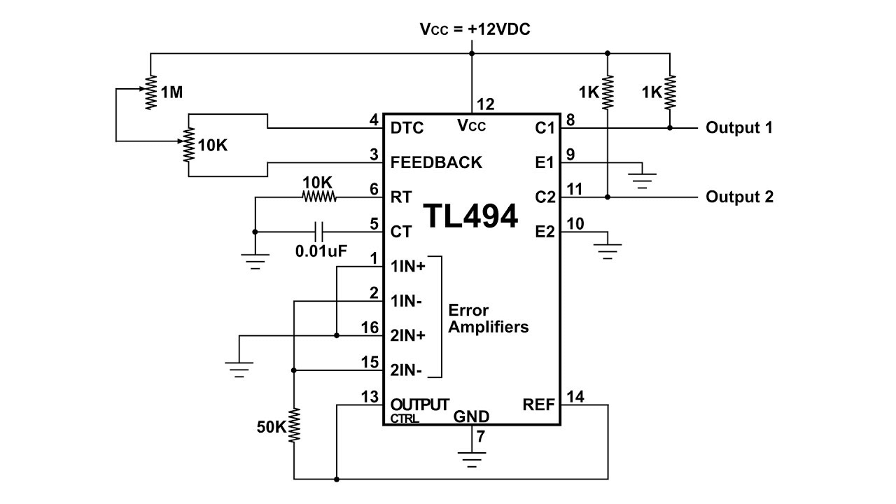
Figure 4: TL494 Control Circuit
Error Amplifiers
The TL494 includes two error amplifiers that regulate output by adjusting their gain in response to varying input conditions. These amplifiers can be powered directly from the supply voltage, allowing them to handle a broad input range. They serve to fine-tune the PWM output, providing stable current by delivering power only when required.
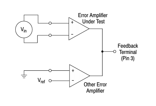
Figure 5: Error−Amplifier
Output-Control Mode
The output-control pin allows for flexible configuration of the output transistors. You can choose between two operating modes: single-ended mode, where both outputs work simultaneously, or push-pull mode, where the outputs alternate. This setting is adjusted without affecting other elements of the TL494, such as the flip-flop or the oscillator, simple change to the mode depending on application requirements.
Output Transistors
The output stage of the TL494 consists of transistors capable of switching up to 200mA of current. These transistors can either source or sink current, depending on the circuit's needs. In common-emitter configuration, the voltage drop across the transistor is less than 1.3V, while in common-collector configuration, the drop is under 2.5V. This output handling allows the TL494 to drive a range of loads with minimal power loss.
5V Reference Source
The TL494 features an internal 5V reference voltage that remains stable as long as the VCC input is above 7V (within a margin of 100mV). This reference voltage is made available through pin 14, labeled REF. It serves as a reliable source for other parts of the circuit, and consistent operation regardless of fluctuations in the input voltage.
Operational Amplifiers
The TL494 is equipped with two operational amplifiers that are powered by a single supply rail. These amplifiers are designed to operate within specific voltage limits, ensuring their output doesn't exceed the system's capacity. Each amplifier has its output connected to a diode, which then links to the COMP pin. This arrangement allows the more active amplifier to dominate the signal passed through the COMP pin, in turn controls the next stage of the circuit.
Sawtooth Oscillator
One feature of the TL494 is its built-in sawtooth oscillator. This oscillator generates a repetitive waveform that fluctuates between 0.3V and 3V. By attaching an external resistor (Rt) and capacitor (Ct), the frequency of this oscillation can be adjusted. The frequency is determined by the formula:
![]()
where ![]() is measured in ohms and
is measured in ohms and ![]() in farads. This tunable oscillator forms the basis for the pulse-width modulation (PWM) timing.
in farads. This tunable oscillator forms the basis for the pulse-width modulation (PWM) timing.
Pulse-Width Modulation Trigger
The pulse-width modulation (PWM) trigger relies on the interaction between the falling edge of the comparator's output and the sawtooth oscillator. As the comparator's output transitions, the trigger activates or deactivates one of the output stages, depending on the conditions set by the comparator and the sawtooth waveform.
Comparator Functionality
The comparator in the TL494 compares the input signal, fed from the operational amplifiers through the COMP pin, to the sawtooth oscillator's waveform. When the sawtooth voltage exceeds the comparator's input, the comparator output is driven low (0). When the input is higher than the sawtooth voltage, the output is driven high (1).
Dead-Time Control
Pin 4, labeled Dead-Time Control (DTC), is responsible for setting a minimum off-time between pulses. This dead-time limits the maximum duty cycle to about 45%, or 42% if the DTC pin is grounded. By adjusting the voltage on this pin, the duration of the quiet period between switching events is controlled, and system doesn't overdrive components.
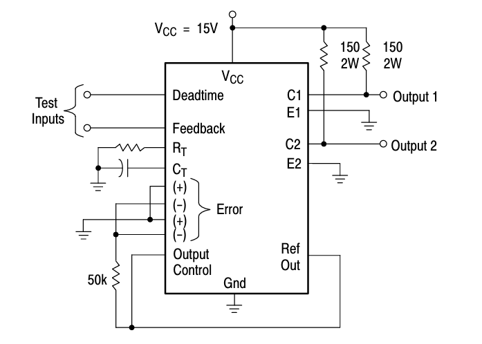
Figure 6: Deadtime and Feedback Control Circuit
Specifications of the TL494
|
Specifications |
Value |
|
Operating Voltage Range |
7V to 40V |
|
Number of Outputs |
2 Outputs |
|
Switching Frequency |
300 kHz |
|
Maximum Duty Cycle |
45% |
|
Output Voltage |
40V |
|
Output Current |
200 mA |
|
Maximum Output Current for Both PWMs |
250 mA |
|
Temperature Range |
-65°C to 150°C |
|
Fall Time |
40 ns |
|
Rise Time |
100 ns |
|
Available Packages |
16-pin PDIP, TSSOP,
SOIC, SOP |
TL494 Recommended Operating Conditions
|
Characteristics |
Symbol |
Min |
Typ |
Max |
Unit |
|
Power Supply Voltage |
VCC |
7 |
15 |
40 |
V |
|
Collector Output Voltage |
VC1, VC2 |
30 |
40 |
V |
|
|
Collector Output Current (Each transistor) |
IC1, IC2 |
200 |
mA |
||
|
Amplified Input Voltage |
Vin |
-0.3 |
|
VCC - 2.0 |
V |
|
Current Into Feedback Terminal |
Ifb |
0.3 |
mA |
||
|
Reference Output Current |
Iref |
10 |
mA |
||
|
Timing Resistor |
RT |
1.8 |
30 |
500 |
kΩ |
|
Timing Capacitor |
CT |
0.0047 |
0.001 |
10 |
µF |
|
Oscillator Frequency |
fosc |
1 |
40 |
200 |
kHz |
Maximum Ratings of the TL494
|
Rating |
Symbol |
Value |
Unit |
|
Power Supply Voltage |
VCC |
42 |
V |
|
Collector Output Voltage |
VC1, VC2 |
42 |
V |
|
Collector Output Current (Each transistor) |
IC1, IC2 |
500 |
mA |
|
Amplifier Input Voltage Range |
VIR |
-0.3 to +42 |
V |
|
Power Dissipation TA ≤ 45°C |
PD |
1000 |
mW |
|
Thermal Resistance, Junction–to–Ambient |
RθJA |
80 |
°C/W |
|
Operating Junction Temperature |
TJ |
125 |
°C |
|
Storage Temperature Range |
Tstg |
-55 to +125 |
°C |
|
Operating Ambient Temperature Range TL494B TL494C TL494I NCV494B |
TA |
-40 to +125 0 to +70 -40 to +85 -40 to +125 |
°C |
|
Derating Ambient Temperature |
TA |
45 |
°C |
Electrical Characteristics of the TL494
|
Characteristics |
Symbol |
Min |
Typ |
Max |
Unit |
|
REFERENCE SECTION |
|||||
|
Reference Voltage (IO = 1.0
mA) |
Vref |
4.75 |
5.0 |
5.25 |
V |
|
Line Regulation (VCC = 7.0 V
to 40 V) |
Regline |
|
2.0 |
25 |
mV |
|
Load Regulation (IO = 1.0 mA
to 10 mA) |
Regload |
|
3.0 |
15 |
mV |
|
Short Circuit Output Current (Vref
= 0 V) |
ISC |
15 |
35 |
75 |
mA |
|
OUTPUT SECTION |
|||||
|
Collector Off−State Current (VCC = 40 V, VCE = 40 V) |
IC(off) |
|
2.0 |
100 |
uA |
|
Emitter Off−State Current VCC = 40 V, VC = 40 V, VE = 0 V) |
IE(off) |
|
|
|
uA |
|
Collector−Emitter Saturation Voltage Common−Emitter (VE = 0 V, IC = 200 mA) Emitter−Follower (VC = 15 V, IE = −200 mA) |
Vsat(C) Vsat(E) |
|
1.1 1.5 |
1.3 2.5 |
V |
|
Output Control Pin Current Low State (VOC˂ 0.4 V) High State (VOC = Vref) |
IOCL IOCH |
|
10 0.2 |
- 3.5 |
uA mA |
|
Output Voltage Rise Time Common−Emitter Emitter−Follower |
tr |
|
100 100 |
200 200 |
ns |
|
Output Voltage Fall Time Common−Emitter Emitter−Follower |
tf |
|
25 40 |
100 100 |
ns |
|
ERROR AMPLIFIER SECTION |
|||||
|
Input Offset Voltage |
VIO |
|
2 |
10 |
mV |
|
Input Offset Current |
IIO |
|
5 |
250 |
nA |
|
Input Bias Current |
IIB |
|
-0.1 |
-1.0 |
uA |
|
Input Common Mode Voltage Range |
VICR |
-0.3
to VCC -2.0 |
V |
||
|
Open Loop Voltage Gain |
AVOL |
70 |
95 |
|
dB |
|
Unity–Gain Crossover Frequency |
fC- |
|
350 |
|
kHz |
|
Phase Margin at Unity–Gain |
φm |
|
65 |
|
deg. |
|
Common Mode Rejection Ratio |
CMRR |
65 |
90 |
|
dB |
|
Power Supply Rejection Ratio |
PSRR |
|
100 |
|
dB |
|
Output Sink Current |
IO- |
0.3 |
0.7 |
|
mA |
|
Output Source Current |
IO+ |
2 |
-4 |
|
mA |
|
PWM COMPARATOR SECTION |
|||||
|
Input Threshold Voltage |
VTH |
|
2.5 |
4.5 |
V |
|
Input Sink Current |
II− |
0.3 |
0.7 |
|
mA |
|
DEADTIME CONTROL SECTION |
|||||
|
Input Bias Current |
IIB (DT) |
|
−2.0 |
−10 |
|
|
Maximum Duty Cycle, Each Output, Push−Pull Mode |
DCmax |
45 |
48 45 |
50 50 |
|
|
Input Threshold Voltage (Zero Duty Cycle) (Maximum Duty Cycle |
Vth |
- 0 |
2.8 - |
3.3 - |
V |
|
OSCILLATOR SECTION |
|||||
|
Frequency |
fosc |
|
40 |
- |
kHz |
|
Standard Deviation of Frequency |
ofosc |
|
3.0 |
- |
% |
|
Frequency Change with Voltage |
Δfosc (ΔV) |
|
0.1 |
- |
% |
|
Frequency Change with Temperature |
Δfosc (ΔT) |
|
- |
12 |
% |
|
UNDERVOLTAGE LOCKOUT SECTION |
|||||
|
Turn−On Threshold |
Vth |
5.5 |
6.43 |
7.0 |
V |
How to Use TL494?
The TL494 is a simple yet powerful chip that controls the power in electronic circuits. To use it, you first need to connect the ground pin to the inverting input pins, that will help the chip receive signals for control. Next, attach the non-inverting input pins directly to the reference voltage pin to provide a stable voltage reference for comparison. To further set up the chip, you'll need to connect the DTC (Dead Time Control) pin and the Feedback pin, to help control the switching speed and test the output, ensuring the chip is working correctly. To control how fast the TL494 switches on and off, you need to connect a capacitor to Pin 5 and a resistor to Pin 6, which together determine the oscillator frequency. Finally, the TL494 includes an error amplifier that checks if the output voltage, typically 5V, matches the reference voltage. If it doesn’t, the amplifier adjusts the pulse-width modulation (PWM) to keep the output steady. With this setup, you can create a basic test circuit and use the TL494 effectively.
How Does a PWM Controller Works?
A PWM (Pulse Width Modulation) controller like the TL494 helps control power by turning signals on and off very quickly. This process allows it to control how much power is sent to a device. The feature of this controller is that it can adjust how long the signal stays on, called the "duty cycle", while keeping the speed or frequency of the signals the same.
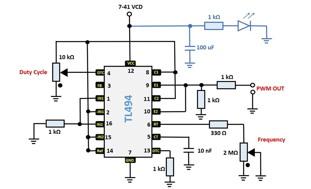
Figure 7: TL494 Pulse Width Modulation Control Circuit
The best part is, you don't need a lot of extra parts to make it work, just a few basic components like resistors and capacitors. Inside the controller, there's something called an oscillator that creates a special wave pattern, called a sawtooth waveform. This wave is compared with other signals from error detectors inside the controller.
If the sawtooth wave is higher than the error signal, the controller sends a signal to turn the power on. If it's lower, it keeps the power off. By doing this, the PWM controller can control how much power is delivered to different parts of an electronic circuit, making it more efficient.
Oscillator Frequency
The frequency of the oscillator in the TL494 chip affects how the waveform (a sawtooth shape) is created. This waveform controls how the PWM (pulse-width modulation) outputs behave that impacts the overall performance of the circuit.
The frequency is set by picking the right values for two parts: the timing resistor (RT) and the timing capacitor (CT). Choosing these parts, you can control the frequency to match what you need. There's a simple formula for this:
![]()
You can control how fast the PWM controller switches on and off by changing the values of RT and CT.
TL494 Circuit Diagram
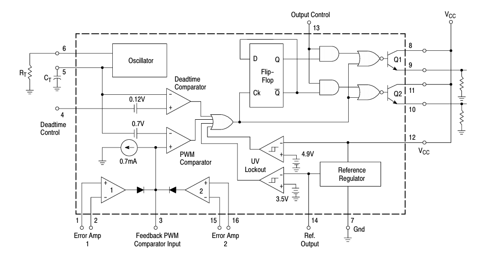
Figure 8: TL494 Circuit
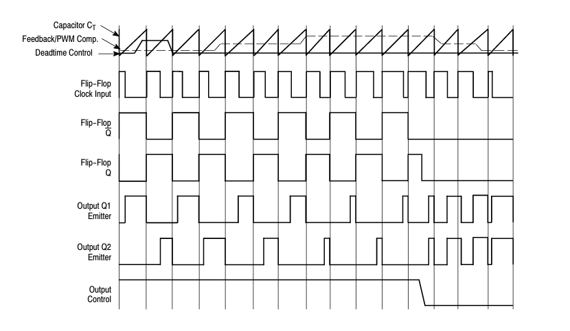
Figure 9: Timing Diagram
Examples of Circuits Using the TL494
TL494 Solar Charger
A solar charger circuit can be built using the TL494 to create a steady 5V power supply, perfect for charging devices. The circuit operates through both voltage and current control. It ensures that the output remains at a stable 5V, providing your devices with the correct voltage. It regulates the current to prevent it from becoming too high, protecting the circuit from potential damage. This type of charger is used for solar-powered applications, helping to save energy and protect your devices.
TL494 Inverter Circuit
An inverter changes DC power (like from a battery) into AC power (like what you use in your home). The TL494 can be used to make an efficient inverter circuit that provides stable power, even when the load (devices connected) changes. In this setup, the TL494 switches the power back and forth quickly, making the conversion from DC to AC smoother. This is useful in home inverters or emergency power systems.
TL494 DC to DC Converter
A DC to DC converter takes one voltage and turns it into another. For example, you can use the TL494 to change 12V DC (like from a car battery) to 5V DC, great for charging USB devices. This circuit has several components that contribute to its functionality. The feedback loop ensures that the output voltage remains steady, while the frequency control adjusts the switching speed to maximize efficiency. The circuit includes protection features that safeguard it by preventing excessive current flow and shutting down in case of overheating. Overall, this type of circuit is ideal for powering small electronic devices.
TL494 Variable Frequency Drive (VFD)
A Variable Frequency Drive (VFD) is used to control the speed of motors. With the TL494, you can build a VFD that adjusts the frequency of power sent to a motor, helping it run at different speeds. This is good for saving energy and extending the life of the motor. The TL494 uses PWM control to generate a special signal that regulates the amount of power sent to the motor. A feedback system continuously monitors the motor's performance and adjusts the power to ensure smooth operation. Variable Frequency Drives (VFDs) are employed in machines such as conveyor belts or fans.
TL494 LED Dimmer
The TL494 can also be used to dim LEDs for lighting systems where adjustable brightness is required. This circuit can be used in homes, cars, or displays. The dimming control adjusts the brightness of the LEDs by modifying the PWM signal. Smooth operation prevents the LEDs from flickering during the dimming process, providing a consistent and stable output. Built-in safety features protect the LEDs from overheating that helps extend their lifespan. Though simple in design, this type of circuit is highly effective for creating energy-efficient lighting systems.
TL494 Equivalent and Alternatives
The UC3843 and TL3842 are very similar to the TL494 in how they work. These chips can often be swapped in power supply and DC-DC converter designs because their switching features and pin layouts are compatible.
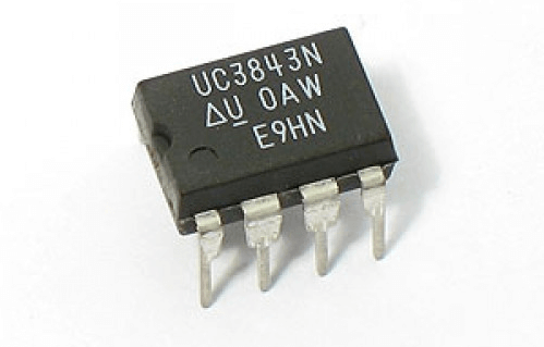
Figure 10: UC3843 Series - UC3843N
The UC2842, while similar to other options, is chosen for different voltage levels or when lower power consumption is required. On the other hand, the SG2524 is another reliable choice, known for its dual in-line packaging and superior performance in more demanding applications.
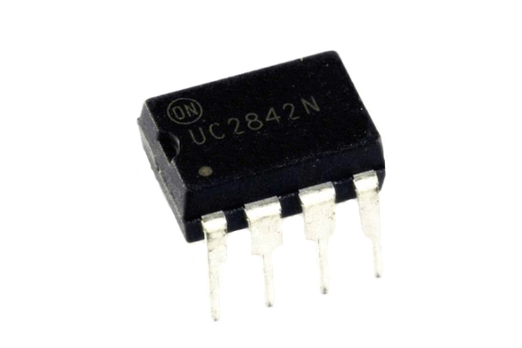
Figure 11: UC2842 Series - UC2842N
TL494 Applications
• LED Lighting Systems
• Battery Chargers
• Automotive Power Systems
• Industrial Motor Controls
• HVAC Systems
• UPS (Uninterruptible Power Supplies)
• Drone Electronics
• Electronic Ballasts for Lighting
• Emergency Lighting Systems
• Consumer Electronics Power Management
TL494 Package
PDIP (Plastic Dual In-Line Package): A through-hole package often chosen for projects where easy soldering and component replacement are important.
SOIC (Small Outline Integrated Circuit): A surface-mount package designed for space-constrained applications, offering a more compact form factor.
TSSOP (Thin Shrink Small Outline Package): Another surface-mount package with a smaller footprint than the SOIC.
SOP (Small Outline Package): Similar to the SOIC, but with slight dimensional variations depending on the specific use case.
Conclusion
The study of the TL494 integrated circuit shows its strong influence on electronic design in power management and control systems. Its flexible design allows it to be adapted for various uses, from simple tasks like dimming LEDs to more complex jobs like controlling industrial motors. Its ability to perform well in tough conditions, thanks to its wide temperature and voltage range, adds to its value in demanding applications. The examples and insights shared here show both the technical strength of the TL494 and its role in driving innovation and efficiency in electronics.
Frequently Asked Questions [FAQ]
1. What is the function of TL494?
The TL494 primary function is to provide precise control of a DC power supply by varying the ratio of on-to-off time in the output signal, controlling the amount of power delivered to a load. It's used in switching power supplies, DC-DC converters, and motor control circuits. Practical operational experience indicates that the TL494 is highly favored for its flexibility in adjusting the duty cycle and frequency to suit various application needs.
2. What is the TL494 constant current regulator?
While the TL494 is known as a PWM controller, it can be configured to act as a constant current regulator. This involves setting up the circuit to deliver a steady current regardless of changes in load or input voltage. This is useful in LED driving applications. Operators often use external components like sense resistors in the feedback loop to stabilize the current, ensuring the longevity and consistent performance of LEDs.
3. What is the duty cycle of TL494?
The duty cycle of the TL494 can be varied from 0% to 100%, though practically, it is often limited to a maximum of about 45% to 90% due to internal circuit limitations. The duty cycle is a parameter that controls the ratio of the "on" time to the total period of the PWM signal, affecting the output voltage and power in applications. Adjusting the duty cycle is a common task for technicians, who might use it to fine-tune the power output in power supplies to match specific load requirements.
4. What is the maximum frequency of TL494?
The TL494 can operate at a maximum switching frequency of around 300 kHz. This high frequency capability allows for smaller size and lower cost of passive components like inductors and capacitors that is a substantial practical advantage in compact power supply designs. Technicians often push the frequency to its upper limits in applications requiring compact and efficient power supplies, balancing between efficiency and the thermal and electronic noise considerations.
5. What is the difference between TL494 and KA7500?
The TL494 and KA7500 are similar in functionality as both are PWM controller ICs. However, they differ slightly in their electrical characteristics and pin configuration. One practical difference is that the KA7500 is cited as having better stability at higher frequencies. Both chips are interchangeable in most applications, and the choice between them usually comes down to availability and cost considerations.
6. What is the feedback pin in TL494?
The feedback pin in the TL494 is implementing voltage or current regulation. This pin is used to sample the output and adjust the PWM duty cycle accordingly, allowing the output stays within desired specifications. Operators connect this pin through a network of resistors or directly to a voltage divider or current sense circuit to provide real-time feedback to the controller. Adjustments to the feedback circuitry are during the initial setup to calibrate the output according to specific application requirements.
7. What is the frequency of TL494 switching?
The switching frequency of the TL494 can go up to 300 kHz. This frequency determines how fast the PWM signal toggles between its high and low states. Setting the switching frequency involves adjusting internal timers or external components that directly affects the efficiency and performance of the entire power supply.