SN74LVC4245APWR Specifications and Applications: Everything You Need to Know
Catalog
SN74LVC4245APWR is a bi-directional bus converter with 8-bit width produced by Texas Instruments. It uses low-voltage CMOS technology and is characterized by low power consumption, high speed and wide operating voltage range. This device is widely used in communication equipment, digital systems, computer peripherals and other areas. In this article, we will provide a detailed description of the parameters and performance of the SN74LVC4245APWR.
SN74LVC4245APWR Overview
The SN74LVC4245APWR is a non-inverting eight-way bus transceiver and a 3.3V to 5V level shifter with three-state output. This device is designed for asynchronous communication between data buses. Depending on the logic level of the direction control (DIR) input, the SN74LVC4245APWR is able to transfer data from the A bus to the B bus, or from the B bus to the A bus. The output enable input allows the user to optionally disable the device, effectively isolating the bus.
The SN74LVC4245APWR supports bidirectional data transfer between two independent levels and has a wide input and output voltage range from 1.65V to 5.5V, making it compatible with a variety of logic families. The device is equipped with 8 independent input/output ports, each of which can be individually configured as input or output mode. Switching between ports is controlled by control pins, which gives the SN74LVC4245APWR a high degree of flexibility and ease of use. In addition, the SN74LVC4245APWR features level shifting and current limiting functions that protect the input/output ports from overvoltage or undervoltage. At the same time, the device also has over-current and short-circuit protection functions to ensure that the device itself will not be damaged when an external fault occurs. These protection measures enable the SN74LVC4245APWR to maintain stable performance in complex working environments.
Alternatives and equivalents:
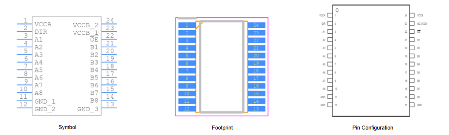
SN74LVC4245APWR Symbol, Footprint and Pin Configuration
SN74LVC4245APWR Power Supply Recommendations
TI level-translation devices offer an opportunity for successful mixed-voltage signal design. A proper power-up sequence always should be followed to avoid excessive supply current, bus contention, oscillations, or other anomalies caused by improperly biased device terminals. Take these precautions to guard against such powerup problems:
Tie OE to VCCA with a pullup resistor so that it ramps with VCCA.
Connect ground before any supply voltage is applied.
Power up the control side of the device (VCCA for all four of these devices).
Depending on the direction of the data path, DIR can be high or low. If DIR high is needed (A data to B bus), ramp it with VCCA. Otherwise, keep DIR low.
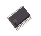
SN74LVC4245APWR Specifications
• SN74LVC4245APWR belongs to the category of bus transceivers.
• The manufacturer of SN74LVC4245APWR is Texas Instruments.
• SN74LVC4245APWR has 8 circuits and 8 channels.
• Its propagation delay time is 6.7 ns.
• It will be shipped in tape and reel packaging to allow for quick mounting and safe delivery.
• Its minimum operating supply voltage of 2.7/4.5 V, while its maximum is 3.6/5.5 V.
• This level shifter has a minimum operating temperature of -40°C and a maximum of 85°C.
• Its low-level output current is 24 mA and high-level output current is -24 mA.
• The SN74LVC4245APWR has a length of 7.8 mm, a width of 4.4 mm, and a height of 1.15 mm.
How to Use SN74LVC4245APWR?
The following are the general steps for using the SN74LVC4245APWR:
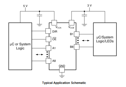
Power connection: First, make sure to provide appropriate power to the SN74LVC4245APWR. The device has two independent power rails, the B port has VCCB, set to 3.3V, and the A port has VCCA, set to 5V. In this way, it allows conversion from a 3.3V environment to a 5V environment and vice versa.
Data bus connection: We connect the A bus and B bus to the corresponding ports of SN74LVC4245APWR respectively. These buses are channels used to transmit data.
Direction control: We control the direction of data transmission through the DIR (direction control) input terminal. The logic level of DIR determines whether data is transferred from the A bus to the B bus, or from the B bus to the A bus.
Pin configuration: We use pins 2 to 11 and pin 14 to 23 of the SN74LVC4245APWR to configure the data path. These pins are aligned with the traditional '245 terminal outputs, allowing designers the flexibility to configure them as needed.
Level conversion: SN74LVC4245APWR has a level conversion circuit that can automatically convert the level of the input port to the level of the output port and vice versa. This ensures correct communication between devices operating in different voltage environments.
Protection circuit: The device also contains current limiting circuit, over-current and short-circuit protection circuit to protect the input/output ports from damage. Under abnormal conditions, these protection circuits work automatically to prevent further damage to the equipment.
SN74LVC4245APWR Application Information
The SN74LVC4245APWR device pinout allows the designer to switch to a normal all-3.3-V or all-5-V 20-pin '245 device without board re-layout. The designer uses the data paths for pins 2 to 11 and pin 14 to 23 of the SN74LVC4245APWR to align with the conventional SN74LVC4245APWR device's pinout. SN74LVC4245APWR is a high drive CMOS device that can be used for a multitude of bus interface type applications where output drive or PCB trace length is a concern.
SN74LVC4245APWR's New Technologies and Trends
The SN74LVC4245APWR bidirectional level converter will develop in the following direction:
Digital Functions
With the development of digital technology, the future SN74LVC4245APWR may add more digital functions, such as I2C or SPI interface. These interfaces will make the configuration and control of SN74LVC4245APWR more flexible and convenient. Through the I2C interface, users can easily configure and monitor the SN74LVC4245APWR without additional complex circuitry or programming.
Wider Voltage Compatibility
As technology continues to advance, voltage standards between different devices and systems are becoming increasingly diverse. In order to meet the communication needs between these devices with different voltage standards, the future SN74LVC4245APWR may expand its input and output voltage range to cover a wider voltage range. It will be able to seamlessly connect devices of different voltage standards, whether the voltage of these devices is higher or lower than the traditional 3.3V or 5V levels. This will greatly improve system flexibility and compatibility, making it easier for designers to build complex multi-level systems.
Integrate Additional Functions
In addition to basic level conversion functions, the new SN74LVC4245APWR may integrate additional functions, such as voltage monitoring, fault detection and diagnostic functions, to improve system reliability and fault tolerance.
Smaller Size and Higher Integration
As the size of electronic devices continues to shrink, future SN74LVC4245APWR may adopt smaller size packages and higher integration designs. A smaller package not only takes up less space, but also further improves the overall performance of the system. By using advanced packaging processes and materials, the SN74LVC4245APWR can achieve a smaller size to meet the needs of compact designs. Higher-integrated designs can integrate more functions into a single chip, which not only helps reduce the number of components required, but also reduces system complexity and cost.
Low-Power Design
With the popularity of mobile devices and portable electronic products, the demand for low-power design is growing. To meet this demand, the new SN74LVC4245APWR may feature a more energy-efficient design aimed at extending battery life and reducing power consumption. For example, it may introduce an intelligent power management function that monitors data transmission on the bus in real time and intelligently adjusts the chip's working status according to actual needs to achieve more refined and efficient power consumption control.
Higher Speed and Bandwidth
As the speed of digital communication continues to increase, the demand for bidirectional level converters is also increasing. Future versions of the SN74LVC4245APWR may provide higher speeds and bandwidth to meet high-speed data transmission requirements.
High Temperature and Industrial Grade Version
As the demand in fields such as industrial automation and automotive electronics increases, the demand for high temperature and industrial grade bidirectional level converters is also increasing, so the future SN74LVC4245APWR may be launched more suitable for versions for high temperature environments and industrial scenes. The new high-temperature and industrial-grade SN74LVC4245APWR will have excellent high-temperature resistance and can maintain stable performance under extreme temperature conditions.
Frequently Asked Questions [FAQ]
1. What is a level converter?
The logic level converter (also called as level shifter, level translator) )is a small device that safely steps down 5V signals to 3.3V and steps up 3.3V to 5V. Each level converter has the capability of converting 4 pins on the high side to 4 pins on the low side. Two inputs and two outputs are provided for each side.
2. What is the replacement and equivalent of SN74LVC4245APWR?
You can replace the SN74LVC4245APWR with SN74LVC4245ADWR, SN74LVC4245APW or SN74LVC4245APWT.
3. What is the SN74LVC4245APWR?
The SN74LVC4245APWR is a octal bus transceiver designed for asynchronous two-way communication between data buses.
4. What is the primary function of SN74LVC4245APWR?
Its primary function is to facilitate bidirectional voltage-level translation and signal buffering between different buses or systems.