Silicon Carbide Unveiled: Properties, Methods and Applications
This article explores the unique qualities of SiC, including its structure, heat resistance, chemical stability, and mechanical strength, which make it better than traditional materials like silicon, gallium nitride, and germanium. It also looks into different ways SiC is produced such as the Acheson Process, Chemical Vapor Deposition, and the Modified Lely Process and how these methods improve its purity and performance for industrial purposes. The article also compares SiC's electrical, thermal, and mechanical properties with other semiconductors, highlighting its increasing use in markets that need high power density, thermal efficiency, and durability.Catalog
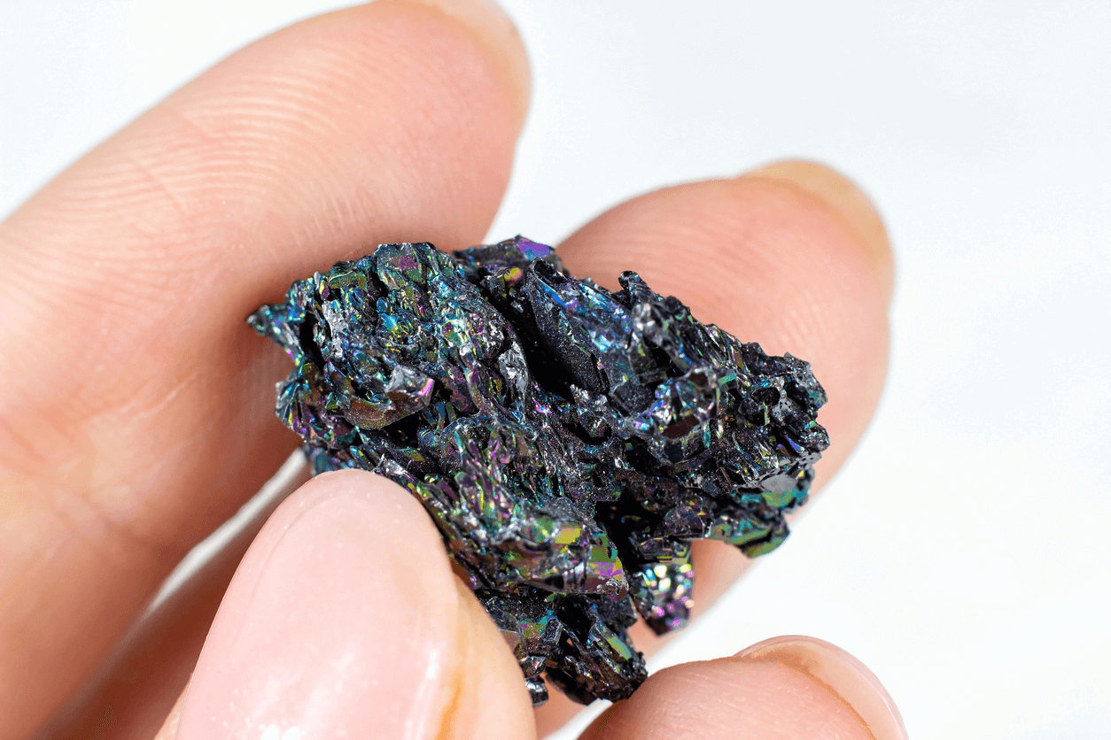
Figure 1: A Closeup of a Woman's Hand Holding a Silicon Carbide (SiC) crystal (aka Carborundum or Moissanite)
Silicon Carbide (SiC) Properties
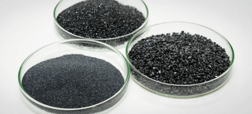
Figure 2: Silicon Carbide in Petri Dish
The most common form of silicon carbide is alpha silicon carbide (α-SiC). It forms at temperatures over 1,700 °C and has a hexagonal crystal shape like Wurtzite. When the temperature is below 1,700 °C, beta silicon carbide (β-SiC) is produced. This version has a crystal structure similar to that of a diamond.
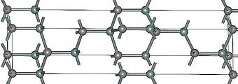
Figure 3: Alpha Silicon Carbide (α-SiC)
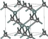
Figure 4: Beta Silicon Carbide (β-SiC)
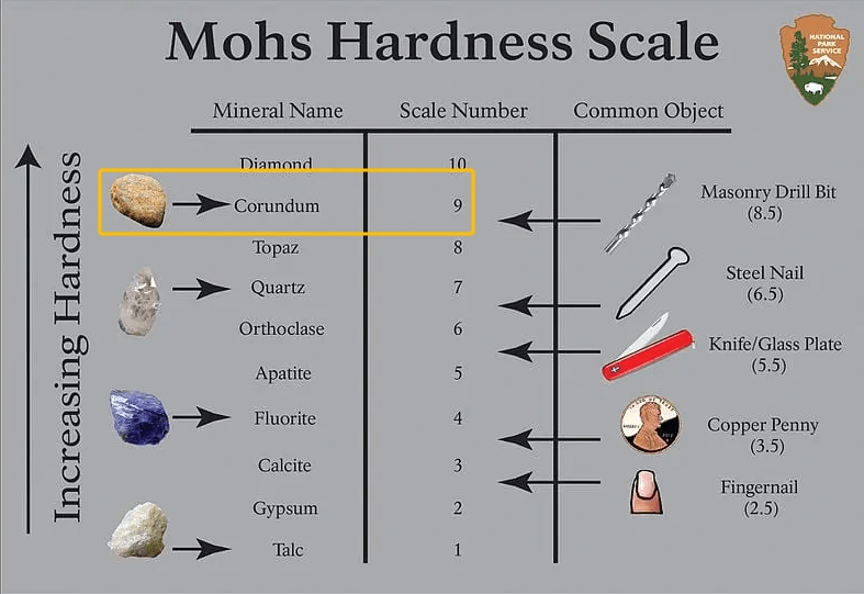
Figure 5: The Mohs Hardness Scale
Silicon carbide is one of the hardest materials after diamond, with a Mohs hardness of about 9 to 9.5. Its Knoop hardness can vary based on its form and purity, but it’s generally very high, often between 2,480 and 3,000 kg/mm².
Silicon carbide can withstand very high pressure, often over 3,000 MPa, has a high bending strength, usually between 400 and 500 MPa, and has a good pulling strength, between 250 and 410 MPa.
|
Hardness
Testing Methods |
Test
Value Range |
Specific
Values (Black Silicon Carbide) |
Specific
Values (Green Silicon Carbide) |
|
Brinell Hardness |
2400-2800 HBS |
2400-2600 HBS |
2600-2800 HBS |
|
Vickers Hardness |
2800-3400 HV |
2800-3200 HV |
3100-3400 HV |
|
Rockwell Hardness |
- |
83-87 HRA |
87-92 HRA |
|
Mohs Hardness |
9-9.5 |
9.2-9.3 |
9.4-9.5 |
SiC conducts heat well, with a thermal conductivity of about 120 W/mK, making it great for managing heat in electronics. At 20°C, it conducts heat at about 0.41 watts per centimeter per degree Celsius (W/cm°C). But when the temperature goes up to 1000°C, its heat conduction drops to around 0.21 W/cm°C.
Furthermore, silicon carbide (SiC) is quickly affected by most metals, metal oxide melts, and alkaline melts, but it does not dissolve in acids or bases. The impurities in technical silicon carbide usually include free carbon (C) and silicon dioxide (SiO2), with small amounts of silicon (Si), iron (Fe), aluminum (Al), and calcium (Ca). The molecular weight of SiC is 40.096. Pure SiC is made of 70.05% silicon (Si) and 29.95% carbon (C).

Figure 6: Silicon Carbide (SiC) Chemical Structure
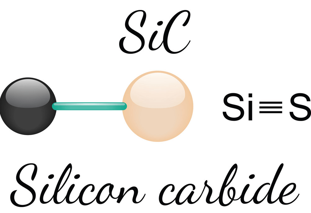
Figure 7: Silicon Carbide (SiC) Chemical Structure
Properties of N-type and P-type Silicon Carbide (SiC)
N-type Silicon Carbide (SiC)
Silicon Carbide (SiC) is a tough material used in high-stress applications because it handles heat well and is very strong. To make N-type SiC, impurities are added, a process called doping, which changes its electrical properties. Elements like nitrogen or phosphorus, which have more valence electrons than silicon, are added to increase the number of free electrons in the SiC structure. This creates a negatively charged, or "n-type," material.
These free electrons greatly improve the electrical conductivity of SiC. In n-type SiC, electrons can move more easily compared to pure SiC, where their movement is limited. This better electron movement makes n-type SiC ideal for power electronics and high-frequency devices where fast and efficient electron flow. While n-type SiC has better conductivity, it doesn't conduct electricity as well as metals, maintaining its semi-conductive properties. This balance allows for precise control of electron flow in various electronic devices.
P-type Silicon Carbide (SiC)
P-type Silicon Carbide (SiC) works differently from its n-type version. P-type doping involves adding elements like boron or aluminum, which have fewer valence electrons than silicon. This creates "holes" or spaces where electrons are missing, giving the material a positive charge and making it "p-type." These holes help carry electrical current by allowing positive charges to move.
Why Silicon Carbide (SiC) Preferred?
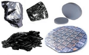
Figure 8: Semiconductor Materials
The table below provides a detailed comparison of four semiconductor materials: Silicon (Si), Gallium Nitride (GaN), Germanium (Ge), and Silicon Carbide (SiC). The comparison is organized into different categories.
|
Aspect |
Silicon
(Si) |
Gallium
Nitride (GaN) |
Germanium
(Ge) |
Silicon
Carbide (SiC) |
|
Electrical Properties |
Mature processes, bandgap of 1.1 eV, limited
in high-power/frequency |
High electron mobility, 3.4 eV bandgap,
high-power/frequency applications |
High electron mobility, 0.66 eV bandgap, high
leakage |
Wide bandgap of 3.2 eV, efficient at high
voltages/temps, low leakage |
|
Thermal Properties |
Moderate thermal conductivity, can limit
high-power uses |
Better than silicon but requires advanced
cooling |
Lower thermal conductivity than silicon |
High thermal conductivity, effective heat
dissipation |
|
Mechanical Properties |
Brittle, sufficient for most uses |
Brittle, prone to cracking on mismatched
substrates |
More brittle than silicon |
Hard, strong, suitable for high-durability
applications |
|
Market Adoption |
Dominant due to established infrastructure
and low cost |
Popular in telecom and defense, limited by
high cost |
Limited due to less favorable properties |
High power density, high temp operation,
efficiency, durability, ongoing cost reduction |
Making Silicon Carbide (SiC)
To make silicon carbide, you usually heat silica sand and carbon-rich stuff like coal to almost 2500 degrees Celsius. This gives you darker silicon carbide with some iron and carbon impurities. Silicon carbide can be synthesized through four main methods, each with distinct benefits tailored for particular uses. These methods include:
Reaction Bonded Silicon Carbide (RBSC)
Reaction-bonded silicon carbide (RBSC) is made from a finely mixed blend of silicon carbide and carbon. The mixture is heated to a high temperature and exposed to liquid or vapor silicon. The silicon and carbon react to form more silicon carbide, and the silicon fills any leftover pores. Like reaction-bonded silicon nitride (RBSN), RBSC changes shape very little during sintering. When these products get to the melting point of silicon, they stay almost as strong as they were before. RBSC is popular in the ceramic industry because it is cost-effective and can be shaped into complex designs.
Figure 9: Reaction Bonded Silicon Carbide
Reaction Bonded Silicon Carbide (RBSC) Procedure:
Combine coarse silicon carbide particles with silicon and plasticizers. Mix until a uniform blend is achieved;
Machine the mixture into the desired shapes and forms. Ensure precision in the geometry to match final specifications;
Place the shaped pieces in a high-temperature furnace. Heat to a temperature that causes a reaction between the silicon and silicon carbide particles;
The silicon reacts with the silicon carbide, bonding to the matrix and increasing strength and durability;
Allow the pieces to cool down gradually to room temperature;
Polish the cooled pieces to meet exact specifications and enhance surface finish.
Modified Lely Process
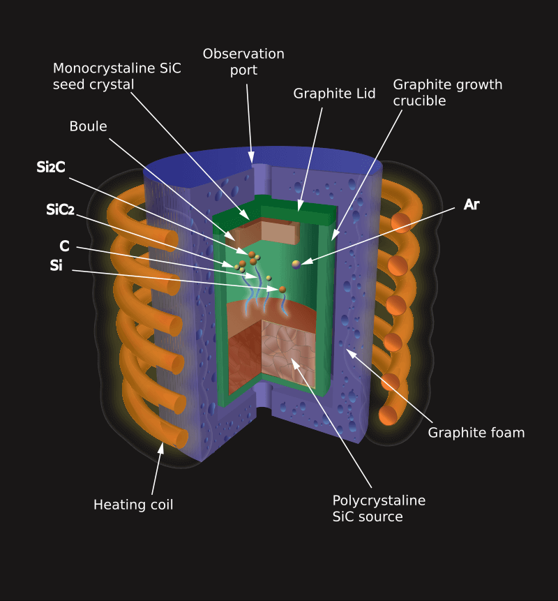
Figure 10: Modified Lely Process
Created in 1978 by Tairov and Tsvetkov, the method is also called the modified-Lely method. The Modified Lely Process improves the synthesis of silicon carbide crystals. It involves heating and then cooling a SiC powder in a semi-closed container, allowing it to form crystals on a seed that is kept at a slightly cooler temperature.
Modified Lely Process Procedure:
Mix silicon and carbon powders thoroughly. Place the mixture in a graphite crucible;
Place the crucible in a furnace. Heat to approximately 2000°C in a vacuum or inert gas environment to prevent oxidation;
The silicon carbide mixture sublimates, changing from a solid to a gas.
Silicon carbide vapors deposit onto a centrally positioned graphite rod. High-purity SiC single crystals form on the rod.
Carefully cool down the system to room temperature.
Extract the high-purity silicon carbide crystals from the graphite rod for use in high-tech applications.
Chemical Vapor Deposition (CVD)
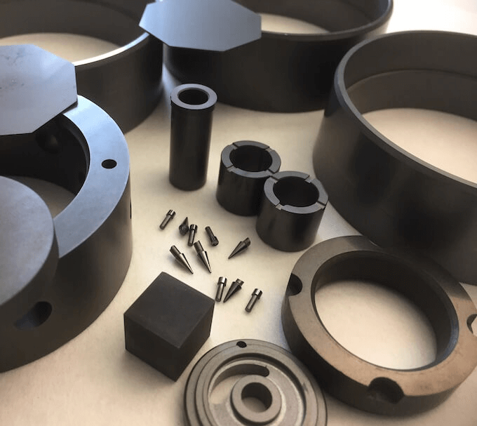
Figure 11: Chemical Vapor Deposition (CVD)
A reactive silane compound, hydrogen, and nitrogen were used in a chemical vapor deposition (CVD) method to produce silicon carbide (SiC) at temperatures between 1073 and 1473 K. By changing the chemical reaction settings, the makeup and hardness of the deposit can be controlled. In the CVD process for silicon carbide, hydrogen and broken-down methyltrichlorosilane (MTS) are mixed on a surface at high temperature and low pressure to create a controlled layer of dense silicon carbide.
Chemical Vapor Deposition (CVD) Procedure:
Prepare silicon tetrachloride (SiCl4) and methane (CH4) as the primary chemical sources;
Place the silicon tetrachloride and methane into a high-temperature reactor;
Heat the reactor to the required temperature to initiate chemical reactions;
The high-temperature environment causes reactions between silicon tetrachloride and methane. These reactions form silicon carbide (SiC);
The silicon carbide forms and deposits onto the desired substrates within the reactor;
Allow the reactor and its contents to cool down gradually;
Extract the coated substrates or components. Conduct any finishing processes to meet final specifications.
The Acheson Process
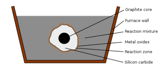
Figure 12: The Acheson Process
The most common way to make SiC is the Acheson method. Edward Goodrich Acheson created this process in 1893 to produce SiC and graphite. Many silicon carbide plants have been using this method ever since.
The Acheson Process Procedure:
Mix silica sand with coke thoroughly;
Arrange the mixture around a central graphite rod in an electric resistance furnace;
Heat the furnace to nearly 2500°C. Maintain the temperature to drive the chemical reaction;
The intense heat causes the silica and carbon to react, forming silicon carbide;
Allow the furnace to cool down gradually;
Extract the formed silicon carbide from the furnace;
Further process the silicon carbide whenever required.
This table provides a simplified comparison of four methods used to produce silicon carbide (SiC). It aims to help understand the unique advantages and best uses of each production technique.
|
Method |
Advantages |
Best
Uses |
|
Reaction Bonded Silicon Carbide (RBSC) |
Makes strong, durable parts Good for complex shapes Little deformation |
Armor plating, high-performance nozzles |
|
Modified Lely Process |
Very pure crystals Perfect structure Better control over the process |
Semiconductors, quantum computing |
|
Chemical Vapor Deposition (CVD) |
Even composition High purity Can use different materials |
Wear-resistant coatings, corrosion-resistant
coatings, semiconductor industry |
|
The Acheson Process |
Simple and low cost Can produce large amounts Consistent, high-quality crystals |
Abrasives, refractory materials |
Silicon Carbide (SiC) in Modern Applications
In the automotive industry, especially for electric vehicles, SiC improves inverter performance and makes battery management systems smaller, extending vehicle range and cutting costs. Goldman Sachs estimates these improvements could save about $2,000 per vehicle.

Figure 13: Silicon Carbide Disk Brake
In solar power, SiC increases inverter efficiency, allowing higher switching speeds, which reduces circuit size and costs. Its durability and stable performance make it better than materials like gallium nitride for solar applications.

Figure 14: SiC for Solar Energy Systems
In telecommunications, SiC excellent thermal management allows devices to handle higher power densities, improving performance in cellular base stations and supporting 5G rollout. These advancements meet the need for better performance and energy efficiency in next-gen wireless communications.

Figure 15: Third-Generation Semiconductor Silicon Carbide
In industrial settings, SiC withstands harsh environments and high voltages, allowing for streamlined designs with less cooling, higher efficiencies, and lower costs, enhancing system performance.
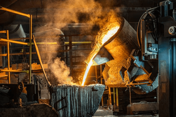
Figure16: Steel Making with Silicon Carbide
In defense and aerospace, SiC is used in radar systems, space vehicles, and aircraft electronics. SiC components are lighter and more efficient than silicon, best for space missions where reducing weight cuts costs.
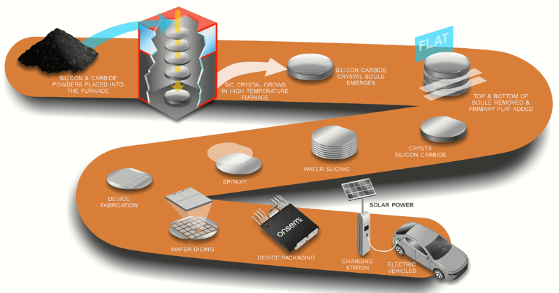
Figure 17: End-to-End SiC Production and Applications
Conclusion
Silicon Carbide (SiC) is becoming the go-to material for many high-demand applications because of its excellent properties and improved production techniques. With its wide bandgap, great thermal conductivity, and strong mechanical properties, SiC is ideal for tough environments that need high power and heat resistance. The article's detailed look at SiC's production methods shows how advancements in material science allow for the customization of SiC properties to meet specific industrial needs. As industries move towards more efficient and compact devices, SiC play a role in automotive, solar power, telecommunications, and aerospace technologies. Ongoing research to reduce costs and improve SiC quality is expected to increase its market presence, reinforcing its important role in the future of semiconductor materials and high-performance applications.
Frequently Asked Questions [FAQ]
1. Who uses silicon carbide?
Silicon carbide is used by industries and professionals working in electronics, automotive, aerospace, and manufacturing. Engineers and technicians rely on it for its durability and efficiency in high-stress environments.
2. What is silicon carbide semiconductor used for?
Silicon carbide semiconductors are used for high-power and high-temperature applications. It is used in power devices for electric vehicles to manage power efficiently, and in diodes and transistors found in renewable energy technologies and high-power applications like railway systems.
3. What is the application of silicon carbide SiC?
Applications of silicon carbide (SiC) include:
Power electronics: Efficient power conversion and management.
Electric vehicles: Enhanced performance and range.
Solar inverters: Increased energy output and reliability.
Aerospace: High-temperature and high-stress components.
Industrial equipment: Strong and long-lasting parts.
4. What products are made from silicon carbide?
Products made from silicon carbide range from semiconductors and electronic devices to abrasives, cutting tools, and heating elements. It's also used in armor and protective gear due to its hardness and thermal resistance.
5. Where is silicon carbide produced?
Silicon carbide is produced in specialized facilities, primarily in the United States, China, and Europe. Companies operate high-temperature furnaces to synthesize SiC from raw materials like quartz sand and petroleum coke.
6. What is the difference between silicon and silicon carbide?
The difference between silicon and silicon carbide lies in their properties and applications. Silicon is a pure element used in standard semiconductor devices and solar panels, while silicon carbide is a compound known for its hardness, high thermal conductivity, and ability to operate at higher voltages and temperatures. This makes SiC ideal for high-power and high-temperature applications, where silicon would fail.