Operational Amplifiers: Inverting Vs Non-Inverting Topologies
An operational amplifier, at its core, is a high-performance voltage amplifier, integral to a myriad of electronic systems. This device pivots on a design philosophy that leverages inductors, capacitors, and resistors. These components intertwine in a dance of sophistication, orchestrating voltage gain via a complex feedback mechanism. Typically, an op-amp is distilled into three fundamental terminals: the inverting input, the noninverting input, and the output. The intricate dance of these terminals dictates the amplifier's performance and application scope.
Catalog

In an idealized scenario, an op amp is a paragon of perfection, boasting attributes like infinite resistance at both inputs—a testament to no current's passage into the terminals. It ensures uniform voltage across inputs, zero output resistance, boundless open-loop gain, infinite bandwidth, and negligible offset. However, before we delve into the realm of operational amplifiers, it is very necessary to understand the nature of negative feedback. This concept isn't merely a pillar in circuit design; it's the cornerstone for high-performance, stable electronic circuits.
Our article aims to unravel the nuances of negative feedback, its design considerations, and the enhancement of circuit performance through its optimization. Next in line is a meticulous dissection of two pivotal operational amplifier topologies: the inverting and non-inverting amplifiers. We delve into their principles, calculation methods, and the pivotal elements in circuit design. This deep dive will afford us a panoramic view of how these amplifier topologies facilitate precision control and unwavering stability in real-world applications.
The Concept and Application of Negative Feedback
Before understanding operational amplifiers (inverting and non-inverting topologies), we need to understand a key concept, negative feedback.
Negative feedback is not only a circuit design technique, but also the cornerstone of achieving high-performance, high-stability electronic circuits. The basic concept of negative feedback is to add a resistor between the output and the inverting input, creating a closed-loop control system.
Detailed Explanation of the Working Principle of Negative Feedback
Op amps can provide extremely high open-loop gains without negative feedback, but such high gains are often accompanied by control difficulties and poor stability.
By introducing a feedback resistor between the output and the inverting input, a portion of the amplifier's output signal is "feedback" back to the input. This method effectively "spreads out" some of the gain, thereby controlling the overall gain of the amplifier.
Design Considerations for Negative Feedback
Selection of feedback resistor: The value of the feedback resistor directly affects the closed-loop gain. Choosing the appropriate resistor value is key to achieving the desired gain and performance.
The relationship between closed-loop gain and bandwidth: The trade-off between gain and bandwidth needs to be considered during design. Increasing the closed-loop gain usually results in a reduction in bandwidth.
Stability and distortion: Appropriate negative feedback can significantly improve the stability of the circuit and reduce signal distortion.
Methods to Optimize Negative Feedback
Accurate calculation of feedback network: By accurately calculating the parameters of feedback resistors and other related circuit components, amplifier performance such as linearity, noise level, and frequency response can be optimized.
Use high-quality electronic components: Choosing high-precision, low-noise resistors, and other components can improve the overall performance of the circuit.
The Impact of Negative Feedback on Circuit Performance
Negative feedback allows for greater stability and better control by sacrificing some of the open-loop gain.
It also helps reduce circuit performance fluctuations caused by external factors such as temperature changes and power supply instability.
Negative feedback is a key technology in operational amplifier design. It achieves gain stability and controllability through fine closed-loop control, which is crucial for improving the overall performance and reliability of electronic circuits. By gaining a deeper understanding of the working principles and applications of negative feedback, electronic circuit designers can design more accurate and stable circuit systems.
Inverting Amplifier Topology Principle and Calculation
In the inverting amplifier topology, the core of the circuit is the operational amplifier, whose inverting input receives the negative feedback signal from the output through the resistor Rf. The characteristic of this topology is that when the output voltage increases, the voltage at the inverting input terminal decreases, thereby reducing the increase in output voltage and forming negative feedback.
In-Depth Analysis of Virtual Short Circuit Status
In an ideal world, we assume that there is no voltage difference between the input terminals of the op-amp, that is, the inverting and non-inverting terminals will be at the same voltage. This state is called a "virtual short circuit".
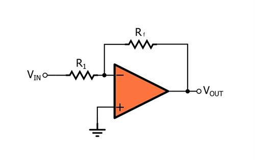
Figure 1: The Inverting Amplifier Topology
Since the non-inverting input terminal is directly connected to the ground (the voltage is 0V), the inverting input terminal must also be kept at 0V to satisfy the virtual short circuit condition.
Detailed Explanation of Anti-Phase Node Analysis
Applying Kirchhoff's current law (KCL) to the inverting terminal, we can derive the following equation:
( 0 − Vin ) / R1 + ( 0 – Vout ) / Rf = 0
Among them, (0 - Vin)/R1 represents the current from the input terminal to the inverting terminal, and (0 - Vout)/Rf represents the current from the output terminal to the inverting terminal.
In-Depth Understanding of Inverting Gain Calculation
By simplifying the above equation, the expression of gain (Vout/Vin) can be obtained:
Vout / Rf = − Vin / R1
Vout / Vin = − Rf / R1
This shows that the magnitude of the gain is determined by the ratio of Rf and R1, and due to the negative sign, the output signal is out of phase (180 degrees out of phase) with the input signal.
Circuit Design Considerations
Input impedance is defined largely by the input resistor R1 in the inverting amplifier. This requires careful consideration of the output impedance of the input signal source for effective impedance matching.
Frequency response, a vital aspect, encounters limitations due to the op amp's inherent bandwidth constraints. This leads to a nuanced balancing act between gain and bandwidth, which must be meticulously optimized to suit the specific application at hand.
Noise and stability, significantly influence circuit performance. The circuit's noise profile, shaped by the resistors and op amps, can be a source of concern. Yet, this is not an insurmountable challenge. By choosing low-noise components and employing a thoughtful circuit layout, these issues can be substantially mitigated.
Non-Inverting Amplifier Topology Principle and Calculation
For the non-inverting amplifier topology, the basic principle is to connect the input signal to the non-inverting input of the operational amplifier, and at the same time use a feedback resistor (Rf) to connect to the non-inverting terminal to form a closed-loop control. In an ideal state, it is assumed that the voltages at the non-inverting input terminal and the inverting input terminal (inverting input) of the operational amplifier are equal, that is, they are zero voltage in the no-signal state. In this case, the voltage at the non-inverting input is equal to the input signal voltage (Vin) because it is directly connected to the input signal.
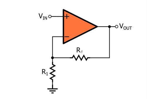
Figure 2: Non-Inverting Amplifier Topology
In-Depth Analysis of In-Phase Node Equations
Applying Kirchhoff's Current Law (KCL) to the inverting terminal, the node equation can be established. This equation takes into account the sum of the currents flowing into the inverting terminal, which must be zero (which can be ignored considering the extremely small input current of the op-amp).
The node equation is as follows:
( Vin – Vout ) / Rf + ( Vin – 0 ) / R1 = 0
Here, (Vin - Vout)/Rf is the current flowing through the feedback resistor to the inverting terminal, and (Vin - 0)/R1 is the current flowing through the input resistor to the inverting terminal.
In-Depth Understanding of Non-Inverting Gain Calculation
By rearranging the above node equations, we can get the relationship between the output voltage (Vout) and the input voltage (Vin):
Vin / Rf + Vin / R1 = Vout / Rf
Further simplification results in:
Vout / Vin = 1 + Rf / R1
This formula shows that the gain of a non-inverting amplifier is determined by the ratio of the feedback resistor to the input resistor and that the gain is at least 1 (i.e. when Rf = 0).
Circuit Design Considerations
Impedance matching: In order to improve the stability of the circuit and reduce signal distortion, the matching of the output impedance of the input signal source and the input impedance of the amplifier should be considered.
Frequency response: Due to the bandwidth limitations of the op-amp, the frequency response of a non-inverting amplifier may decrease as gain increases. Design should consider selecting the appropriate OP amp model and adjusting circuit parameters to meet application requirements.
Noise and Stability: Resistor noise and op-amp internal noise both affect non-inverting amplifier performance. Low-noise resistors and op amps should be selected during the design, and proper routing and grounding strategies should be used to improve the overall stability and noise rejection of the circuit.
Conclusion
By delving deeply into the nuances of negative feedback, inverting amplifier, and non-inverting amplifier topologies, we gain a richer appreciation of their pivotal role in the realm of modern electronic circuit design. Let's first turn our attention to the benefits of negative feedback. It's a game-changer: negative feedback fundamentally bolsters both stability and accuracy in circuits by diminishing gain. Consider, for instance, an operational amplifier. Here, negative feedback is a potent tool, dramatically reducing the output impedance while simultaneously boosting the input impedance. This dual action fine-tunes the circuit's response characteristics. This enhancement is twofold: it not only elevates circuit performance but also remarkably mitigates the effects of temperature fluctuations and device aging on the circuit's efficiency.
Now, let's navigate the intricacies of inverting and non-inverting amplifier topologies. Inverting amplifiers, known for their 180-degree phase inversion between input and output signals, are integral to sound systems and signal processing. Take audio amplifiers as an example; inverting amplifiers are instrumental in delivering a pristine, distortion-free output signal, thus elevating audio quality. On the other hand, non-inverting amplifiers play a crucial role in data acquisition and sensor interfaces, thanks to their phase-aligned input and output. They excel in truncating signal paths and curtailing noise interference, which, in turn, amplifies the system's signal-to-noise ratio.
In essence, this foundational knowledge of electronic circuit design does not merely deepen our understanding of circuitry principles; it establishes a robust platform for creating efficient, low-noise, and adaptable electronic systems. A thorough grasp of these concepts equips electronic designers with a vast canvas for innovation, spurring ongoing advances in electronic technology.