Mastering the Art of Soldering Ball Grid Arrays
The position of efficient and reliable semiconductor packaging cannot be overstated in the rapidly evolving world of electronic device manufacturing. Ball Grid Array (BGA) technology emerges as an ideal solution to meet the growing demands of modern electronics for higher performance and miniaturization. This article digs into the intricate details of BGA technology, exploring its ultimate components, processes, and the technical challenges it addresses in semiconductor packaging. From the basic structure and advantages of BGA over traditional pin-based systems like the quad flat pack to the sophisticated processes of soldering, inspection, and rework, the discourse offers a comprehensive analysis.Catalog
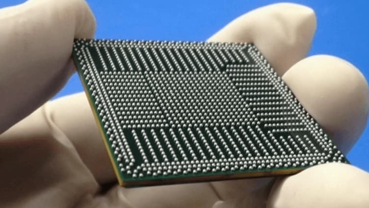
Figure 1: Ball Grid Array
Basics of Ball Grid Arrays
A Ball Grid Array (BGA) is a modern solution in semiconductor packaging, designed to overcome the challenges of older, pin-based methods like the quad flat pack. Instead of using fragile pins, the BGA relies on an array of small solder balls. These balls are precisely positioned on the underside of the package and are meant to connect with matching copper pads on a printed circuit board (PCB). When heated, the solder balls melt and secure the BGA to the board, creating a strong and reliable connection.
The BGA format provides several practical advantages. First, it simplifies the PCB layout by reducing the need for densely packed interconnections that earlier packaging systems required. This more efficient layout makes the BGA more durable and reduces the risk of damage during handling, unlike the delicate pins found in older packages that can bend or break easily.
In addition, the BGA offers superior heat management and electrical efficiency performance. The short, direct connection between the BGA and the PCB helps to dissipate heat more effectively, which helps maintain the stability of circuits under thermal stress. As well, the shorter electrical paths within the BGA reduce signal loss, which is especially substantial for devices operating at high frequencies. This combination of durability, heat dissipation, and electrical efficiency makes BGA packaging an increasingly popular choice for modern electronic devices as their complexity and performance demands grow.
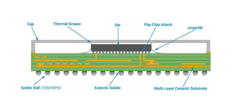
Figure 2: BGA Soldering Process
Navigating the BGA Solder Process
The process of soldering a Ball Grid Array (BGA) was initially questioned due to concerns about its reliability and the difficulty of inspecting the connections hidden underneath the component. Nevertheless, over time, BGA soldering has proven to be more dependable than older systems, like quad flat packs, thanks to precise control during the soldering process. This improved reliability has led to its widespread use in both large-scale manufacturing and smaller, prototype PCB assemblies.
The reflow soldering method is dominant in attaching a BGA to a printed circuit board (PCB). In this process, the entire assembly is heated to a specific temperature where the solder beneath the BGA melts into a semi-liquid state. This stage is carefully controlled to ensure the solder maintains its structure and doesn't cause the solder balls to collapse or merge. Accurate temperature regulation is serious because any fluctuations can affect the quality of the connections.
An extensive feature of the reflow process is the way the molten solder behaves. Its natural surface tension helps pull the BGA into perfect alignment with the PCB pads, even if the component was slightly off-center when placed. This self-correcting ability ensures each connection is properly made without manual adjustments. These advanced techniques not only make BGA soldering highly reliable but also more efficient, helping to make BGA a preferred option in modern circuit board production.
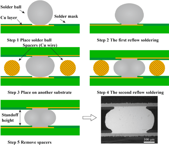
Figure 3: BGA Solder Joint Inspection
How to Inspect BGA Solder Joints Effectively?
Inspecting BGA solder joints is an insistent part of the assembly process, complicated by the fact that the joints are hidden beneath the BGA component. Since traditional visual inspection can't access these concealed connections, X-ray and Automated X-ray Inspection (AXI) techniques are used to get a clear, non-invasive view of the solder joints.
X-ray inspection is useful for thoroughly checking each solder joint. The imaging allows technicians to ensure that all solder balls have melted correctly and formed strong bonds with the PCB. This step is used to identify problems like cold joints, where the solder hasn't fully melted, or voids, which are air pockets that can weaken the joint over time.
Through X-ray technology, inspectors can confirm that the proper amount of heat was applied during the reflow process and that the solder joints meet precise standards. This level of scrutiny ensures that the final product is reliable and able to withstand the operational stresses it may face, helping to maintain high manufacturing quality.
Effective Strategies for BGA Rework in Electronics
Reworking a BGA component is a highly precise task that requires careful control over the heating process. This work is usually done at a specialized rework station equipped with tools designed specifically for the job. Localized infrared heating is used to target the BGA without overheating nearby parts. Once the solder beneath the component melts, a vacuum tool carefully lifts the BGA from the board. Throughout this process, the heat must be controlled precisely to avoid damaging adjacent components, highlighting the need for advanced rework equipment.
Successful BGA rework depends on maintaining accurate temperature settings and controlling the environment around the component. This prevents the surrounding circuitry from being affected during the removal and replacement of a faulty BGA. The task demands a deep understanding of how BGAs function and skilled handling to ensure the process is done correctly. Because of these complexities, BGA rework is a delicate operation that requires both the right equipment and experienced technicians to maintain the integrity of the entire assembly.
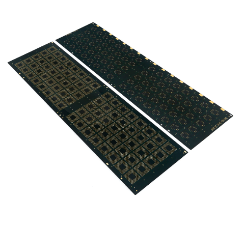
Figure 4: BGA PCB Land Patterns
Design Strategies for BGA PCB Land Patterns
Designing PCB land patterns for BGAs requires precise attention to detail to ensure a smooth and secure connection during assembly. The land patterns must be perfectly aligned with the BGA's grid, ensuring that each solder ball lines up accurately with the corresponding pad. Key design features like solder mask relief, and in some cases, leaving pads uncovered by the mask, are used to allow more solder to flow and create a stronger bond. Strict adherence to IPC standards is useful to achieve the level of accuracy wanted for successful BGA soldering.
Every aspect of the land pattern must be carefully planned to meet the specific requirements of the BGA component. This includes adjusting the size of the pads and carefully managing positional tolerances to make sure each connection is flawless. Thoughtful planning at the design stage ensures that the soldering process is both efficient and reliable, helping the BGA attach securely and function properly within the PCB assembly.
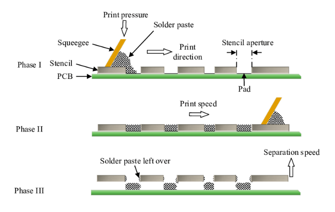
Figure 5: BGA Solder Paste Printing
Achieving Precision in BGA Solder Paste Printing
Applying solder paste for BGA assembly requires precise stenciling techniques to ensure that small, exact amounts of paste are deposited under each BGA ball. This process uses laser-cut stencils that are perfectly aligned with the PCB land patterns. To further improve accuracy and minimize defects like solder balling, these stencils are often treated with nanocoatings. Miniature print heads then carefully control the amount of paste being applied to each pad, while optical verification systems check that the paste is placed with high precision.
The type of solder paste used—typically Type 3 or Type 4—depends on the viscosity wanted for the specific assembly. The choice of paste directly impacts how well the solder joints form during the reflow process. Since this step lays the groundwork for the strength and reliability of the final connections, the solder paste printing process is a dangerous part of BGA assembly, requiring careful attention to detail to ensure high-quality results.
Complexities of BGA Soldering
Soldering BGAs presents unique difficulties because the solder joints are hidden beneath the component, making direct visual inspection impossible. To address this, specialized tools like X-ray machines are used to inspect the connections, while infrared rework stations allow for precise realignment of the component when needed. Managing the soldering process also requires careful control of heat to avoid stressing the solder joints, which can lead to cracks. Similarly, all solder balls must maintain the same height (coplanarity) to ensure consistent performance and long-term reliability.
Environmental factors such as aging and moisture sensitivity further complicate the process. These issues need to be tightly controlled to prevent deterioration of the solder joints over time. Successfully navigating these challenges demands a thorough understanding of BGA soldering techniques and the use of advanced equipment.
Various Types of Ball Grid Arrays
Ball Grid Array (BGA) technology is a method of mounting integrated circuits (ICs) onto printed circuit boards (PCBs) that improves electrical connectivity and heat dissipation. It uses an array of solder balls beneath the component to create secure connections.
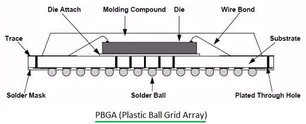
Figure 6: Plastic Ball Grid Arrays (PBGA)
Plastic BGAs are widely used because they are affordable and deliver reliable performance for most standard applications. They consist of a plastic substrate with solder balls attached underneath. These are often found in consumer electronics, automotive systems, and other devices that don't operate under extreme conditions. Their simple design offers good electrical connectivity and moderate heat management, which is sufficient for everyday use.
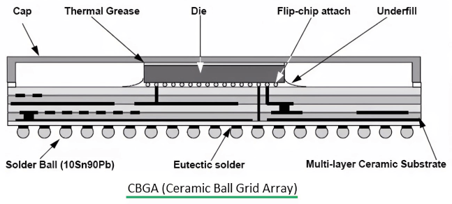
Figure 7: Ceramic Ball Grid Arrays (CBGA)
Ceramic BGAs use a ceramic substrate, making them more resistant to heat and electrical interference than plastic BGAs. This durability makes them ideal for demanding environments like telecommunications, aerospace, and high-end servers. Ceramic provides excellent insulation and can handle both high temperatures and mechanical stress, ensuring the device's long-term reliability.
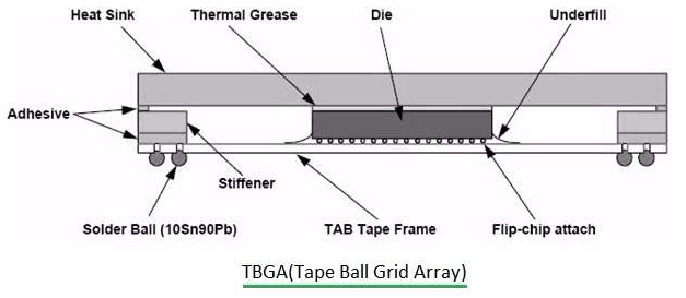
Figure 8: Tape BGAs (TBGA)
Tape BGAs are designed with a flexible substrate that can conform to the surface of the PCB, improving both the mechanical connection and heat dissipation. These BGAs are ideal for portable electronics and high-density devices where space is limited. The flexible nature of the substrate allows for better thermal management in compact spaces, making them a preferred choice for smartphones and other portable devices.
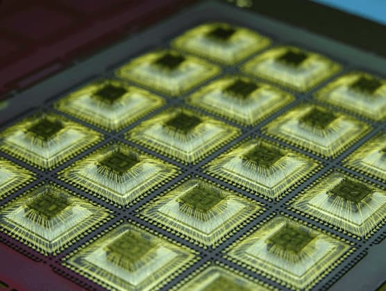
Figure 9: Stacked Die BGAs
Stacked Die BGAs are used in devices that need to pack a lot of processing power into a small space. This type stacks multiple integrated circuits vertically within a single package, allowing for more functionality without increasing the device’s size. Stacked Die BGAs are commonly found in smartphones, tablets, and other compact electronics that require high performance in a small form factor.
Conclusion
The exploration of Ball Grid Array (BGA) technology underscores its key role in the modern electronics manufacturing landscape. As detailed in this article, BGA packaging not only addresses the physical limitations of older packaging methods but also significantly enhances performance through improved heat management and electrical efficiency. The technical processes involved in BGA soldering, inspection, and rework reflect a commitment to precision and reliability, ensuring that electronic devices meet the stringent requirements of today's technological standards.
In addition, the various types of BGAs, from Plastic BGAs to High Thermal Conductivity Metal Top BGAs, cater to a broad spectrum of applications, proving the versatility and adaptability of BGA technology. Ultimately, as electronic devices continue to evolve in complexity and functionality, BGA technology will remain requisite, continuing to drive innovations and maintain high standards of quality in semiconductor packaging.
Frequently Asked Questions [FAQ]
1. How to solder a BGA package?
Preparation: Begin by cleaning the BGA package and the PCB (Printed Circuit Board) to remove any contaminants or residue.
Alignment: Carefully align the BGA package on the PCB, ensuring that all pads on the chip align with the corresponding pads on the board.
Soldering: Utilize a reflow soldering process. Place the PCB with the BGA into a reflow oven. The solder already applied to the pads will melt and form connections during the heating cycle.
Cooling: Allow the PCB to cool slowly after the reflow process to avoid any thermal stress.
2. What is BGA in soldering?
BGA stands for Ball Grid Array. It is a type of surface-mount packaging used for integrated circuits. BGA packages use tiny balls of solder fixed to the underside of the package to establish electrical connections with the PCB instead of traditional leads.
3. How to do ball soldering?
Ball Placement: Apply solder paste to the PCB pads where the BGA will be placed. Position the BGA so that each solder ball aligns with the corresponding pad on the PCB.
Reflow Soldering: Heat the assembly in a reflow oven. The solder paste will melt, bonding the solder balls to the pads and creating a solid electrical and mechanical connection.
Inspection: After soldering, inspect the connections for any bridges or poor joints, typically using X-ray inspection to see beneath the BGA.
4. How to check BGA soldering?
Visual Inspection: Initially, check for any visible misalignment or defects around the BGA package.
X-ray Inspection: Since BGA soldering cannot be fully verified visually due to the hidden nature of the connections, use X-ray inspection to examine the solder joints underneath the BGA.
Functional Testing: Finally, perform electrical testing to ensure all connections are functioning correctly.
5. What temperature should BGA solder be?
Typical Temperatures: The precise temperature for soldering BGA depends on the solder paste used. Typically, lead-free solder paste requires temperatures around 217°C to 245°C. Check the solder paste manufacturer's specifications for exact temperatures.
Reflow Profile: Follow a specific thermal profile that gradually heats the assembly to the required reflow temperature, holds it there long enough to ensure proper solder melting, and then cools it down gradually to avoid thermal stress.