JRC4558 Op-Amp: Features, Specifications, and Applications
The JRC4558 is a flexible dual operational amplifier widely used in electronics. This article explores its features, including stable frequency, wide voltage range, and high-temperature resistance, making it reliable across applications. Compared to amplifiers like the TL072 and NE5532, the JRC4558 is ideal for both simple and advanced projects, found in guitar pedals, audio systems, and medical equipment.Catalog
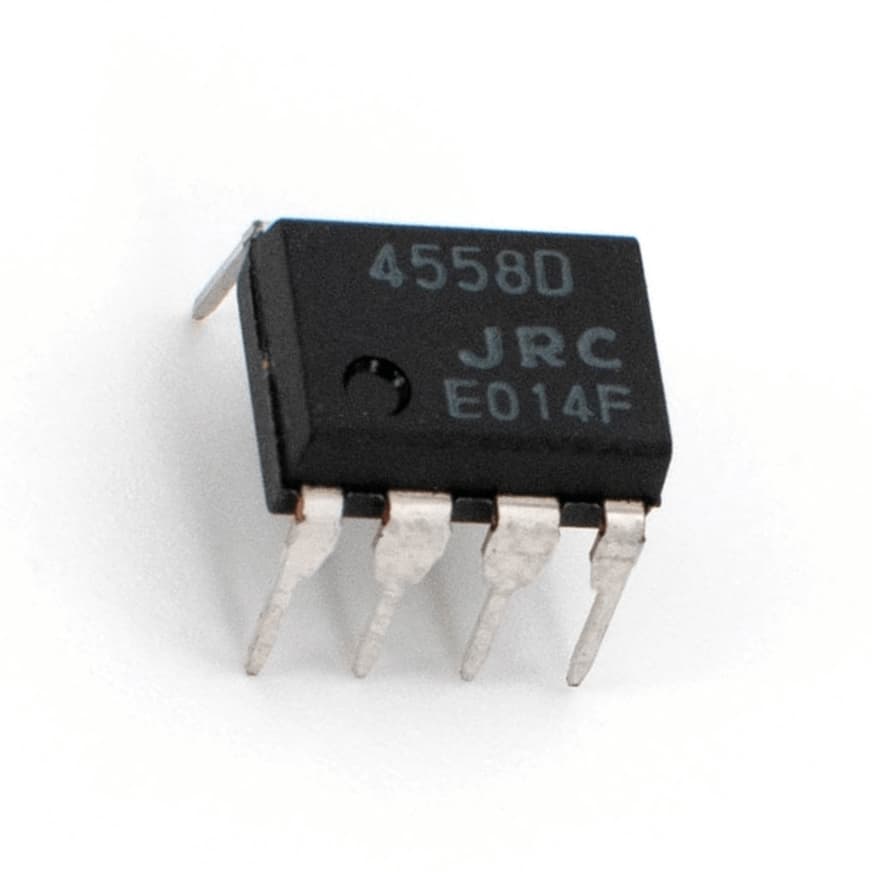
Figure 1: JRC4558 Op-Amp
What Is JRC4558 Op-Amp?
The JRC4558 is a widely used dual operational amplifier (op-amp) with eight pins. It's known for having good input impedance and strong voltage amplification. It comes in two main types: SOP and DIP for different circuit designs. This chip is popular in guitar pedals, offering up to 100 dB of voltage gain and a 5 megaohm input impedance. It operates on a power range between ±4V and 18V. The pin layout of the JRC4558 is simple and it makes circuit design easier. Pin 8 is connected to the positive voltage, and pin 4 to the negative voltage. The outputs of the two amplifiers are found at pins 1 and 7. The inverting inputs, reverse the signal, are on pins 2 and 6, while the non-inverting inputs that keep the signal the same, are on pins 3 and 5.
Each amplifier operates independently, handling different signals simultaneously. The chip has built-in stabilization, managing a wide voltage range effectively. It has high input impedance, means it doesn't draw much current. While the 100 dB gain isn't the highest, it's enough for most uses. The chip also has a fast response time with a slew rate of 1.7V per microsecond. This chip is designed to increase the difference in voltage between its input signals, and useful for tasks like comparing signals or amplifying small differences in voltage. A big advantage is that it can run on just a +5V power supply, unlike other op-amps that need both positive and negative power sources, making it easier to use in simple circuit designs without losing performance.
JRC4558 Features and Specifications
JRC4558 Features
No Frequency Adjustment - The design is stable and doesn't need extra tuning to keep the frequency response steady.
No Risk of Getting Stuck - The system is designed to avoid locking up during use, improving reliability.
Wide Voltage Handling - Works with a range of common and differential voltages, for various circuits.
Consistent Performance in Heat - Measures like gain and offset remain stable even with temperature changes.
Matched Amplifiers - Amplifiers are balanced in gain and phase, reducing performance differences.
Built-in Frequency Optimization - The system is already optimized for frequency, no manual tuning required.
Low-Noise Input - Input design reduces noise, providing a cleaner signal.
Compatible with MC1458/LM358 - Works with standard MC1458 and LM358 chips for easy integration into existing designs.
JRC4558 Specifications
|
JRC4558
Specification |
Details |
|
Supply Voltage Range |
Operates between ±5V and ±15V. |
|
Bandwidth |
3MHz, for a wide range of signal frequencies. |
|
Operating Temperature |
Reliable between 0°C and 70°C. |
|
Slew Rate |
Fast response rate of 1.7V/μs. |
|
Voltage Gain |
Amplifies signals up to 100dB, for high-gain applications. |
|
Package Options |
Available in 8-pin SOP and DIP formats for design flexibility. |
Maximum Ratings of JRC4558
|
Parameter |
Symbol |
Value |
Unit |
|
Supply Voltage |
Vcc |
±22 |
V |
|
Differential Input Voltage |
VI(DIFF) |
±18 |
V |
|
Input Voltage |
VI |
±15 |
V |
|
Operating Temperature |
TOPR |
-20~+85 |
℃ |
|
Power Dissipation (P-DIP) |
PD |
600 |
mW |
|
Power Dissipation (SOP) |
PD |
400 |
mW |
|
Storage Temperature Range |
TSTG |
-65~+150 |
℃ |
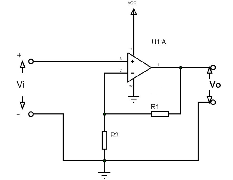
Figure 2: JRC4558 Internal Circuit Diagram
Electrical Characteristics of JRC4558
|
Parameter |
Symbol |
Test Conduction |
Min |
Typ |
Max |
Unit |
|
Supply Current, all Amp, no load |
Icc |
- |
- |
2.3 |
4.5 |
mA |
|
Input offset voltage |
VIO |
Rs<10KΩ |
- |
2 |
6 |
mV |
|
Input offset current |
IIO |
- |
- |
5 |
200 |
nA |
|
Input bias current |
IBIAS |
- |
- |
30 |
500 |
nA |
|
Large signal voltage gain |
GV |
Vo(p-p)= ±10V, RL≤2kΩ |
20 |
200 |
- |
V/mV |
|
Common Mode Input Voltage Range |
VI(R) |
- |
±12 |
±13 |
- |
V |
|
Common Mode Rejection Ratio |
CMRR |
Rs ≤10kΩ |
70 |
90 |
- |
dB |
|
Supply Voltage Rejection Ratio |
PSRR |
Rs ≤10kΩ |
76 |
90 |
- |
dB |
|
Output Voltage swing |
Vo(p-p) |
RL≥10kΩ |
- |
±12 |
±14 |
V |
|
Power Consumption |
Pc |
- |
- |
70 |
170 |
mW |
|
Slew Rate |
SR |
Vi=±10V, RL≥2kΩ,
CL≤100pF |
1.2 |
2.2 |
- |
V/µS |
|
Rise Time |
TRIS |
Vi=±20mV, RL≥2kΩ,
CL≤100pF |
- |
0.3 |
- |
µs |
|
Overshoot |
OS |
Vi=±20mV, RL≥2kΩ,
CL≤100pF |
- |
15 |
- |
% |
|
Input Resistance |
Ri |
- |
0.3 |
2 |
- |
MΩ |
|
Output Resistance |
Ro |
- |
- |
75 |
- |
Ω |
|
Total Harmonic Distortion |
THD |
f=1KHz, Av=20dB, RL=2kΩ,
Vo=2Vpp, CL=100pF |
- |
0.008 |
- |
% |
|
Channel Separation |
Vo1/Vo2 |
- |
- |
120 |
- |
dB |
Frequency Characteristics of JRC4558
|
Parameter |
Symbol |
Test
Condition |
Min |
Typ |
Max |
Unit |
|
Unity Gain Bandwidth |
BW |
- |
2.0 |
2.8 |
- |
MHz |
JRC4558 Pin Configuration
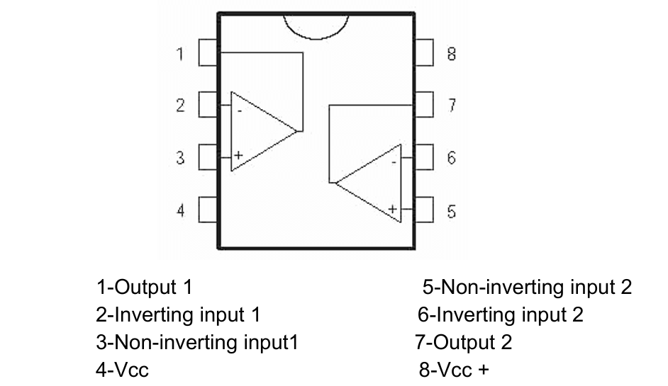
Figure 3: JRC4558 Pinout
|
Pin No. |
Pin Name |
Pin Description |
|
1 |
Output 1 |
The output pin of Op-amp 1 |
|
2 |
Inverting Input 1 |
The inverting input pin of Op-Amp 1 |
|
3 |
Non-Inverting Input 1 |
The non-inverting input pin of Op-Amp 1 |
|
4 |
Vcc |
Negative supply or ground terminal |
|
5 |
Non-Inverting Input 2 |
The non-inverting input pin of Op-Amp 2 |
|
6 |
Inverting Input 2 |
The inverting input pin of Op-Amp 2 |
|
7 |
Output 2 |
The output pin of Op-amp 2 |
|
8 |
Vcc + |
Positive supply terminal |
Amplifying with the JRC4558
The JRC4558 chip is used in audio and signal processing because it can be used in many ways. How it's wired determines the different types of amplification it can do. Here are two simple setups that show how the JRC4558 can boost signals.
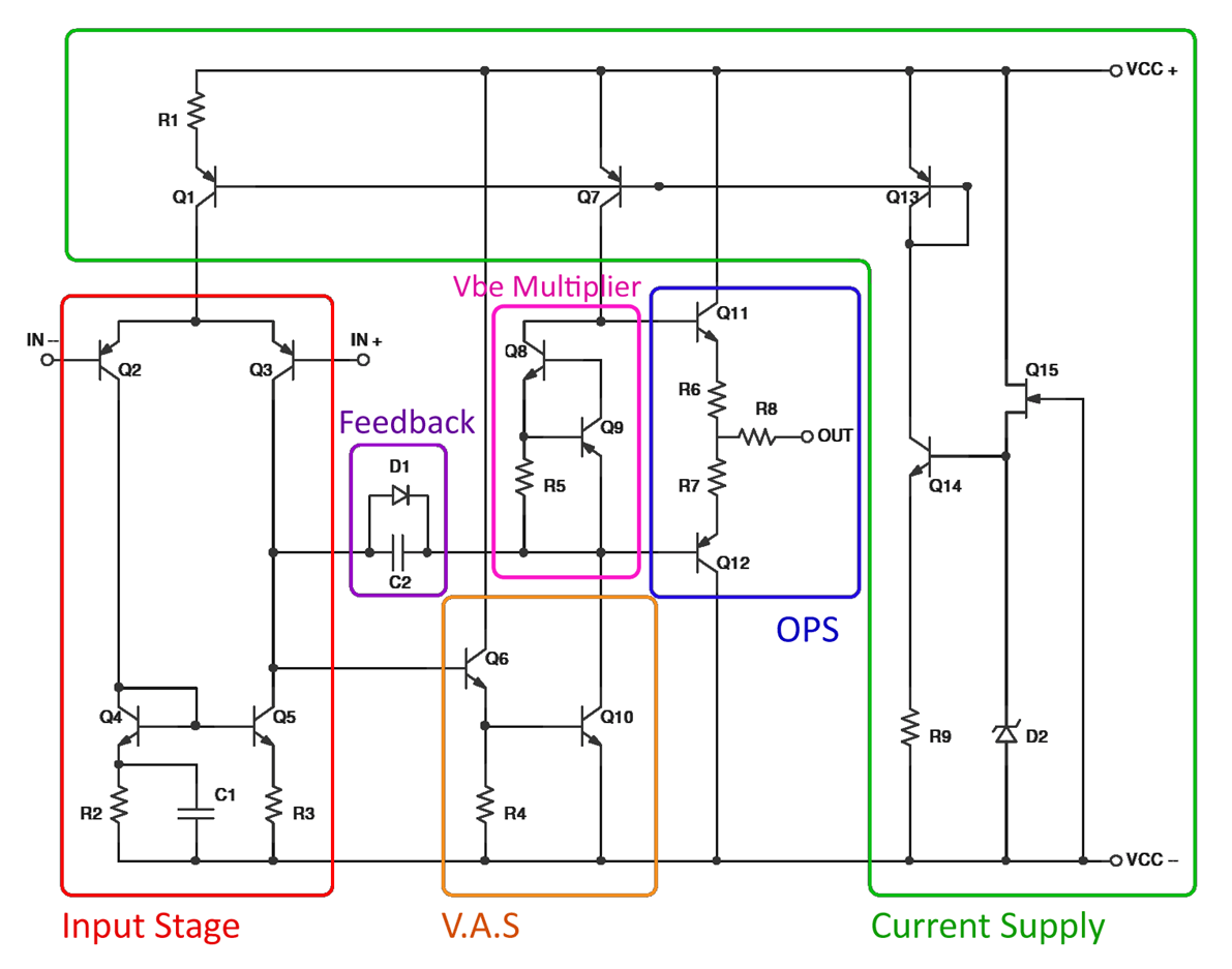
Figure 4: JRC4558 Amplifier Circuit Diagram
Inverting Amplifier Configuration
In the inverting configuration, the input signal is connected to the inverting input (pin 2) of the JRC4558. This setup requires two resistors: one connected between the input signal and the inverting input, and another acting as a feedback resistor between the output and the inverting input.
The main characteristic of this configuration is that the output signal is an inverted version of the input signal. This means the output is the exact opposite of the input, when the input goes positive, the output goes negative, and vice versa. The amount of amplification, or gain, is determined by the ratio of the two resistors. The gain is calculated as the ratio of the feedback resistor (labeled Rf) to the input resistor (Ri) but with a negative sign because of the phase inversion:
![]()
This formula means that if the feedback resistor is larger than the input resistor, the output signal will be amplified but still inverted.
Non-Inverting Amplifier Configuration
In the non-inverting configuration, the input signal is connected to the non-inverting input (pin 3) of the JRC4558. In this arrangement, the output signal remains in phase with the input. This means that if the input signal rises, the output rises in sync with it, maintaining the same polarity.
This setup also requires two resistors: one connected between the output and the inverting input (pin 2), and the other between the inverting input and ground. The gain in this configuration is calculated differently than in the inverting setup. Here, the gain is always greater than or equal to 1, meaning it amplifies the signal without any phase inversion. The gain formula is:
![]()
In this case, the value of the feedback resistor (Rf) and the resistor connected to ground (Ri) determine how much the signal is amplified. The “1” in the formula ensures that even if the resistors are of equal value, the gain is still greater than unity. One benefit of the non-inverting configuration is that it offers a higher input impedance.
JRC4558 Applications

Figure 5: JRC4558 Applications
• Guitar Pedals
The JRC4558 is a main component in guitar pedals, especially in iconic models like the Tube Screamer. It shapes the audio signal to produce a rich, warm, and overdriven tone that is highly sought after by guitarists for its ability to enhance expression in their playing.
• Hi-Fi Systems
In high-fidelity audio systems, the JRC4558 improves sound clarity and depth by refining signals within preamplifiers and audio mixers. Its use helps ensure that listeners experience a more dynamic and immersive sound, enhancing both the highs and lows of the audio spectrum.
• Filters
The chip is part of both high-pass and low-pass filters. These filters manage the range of frequencies allowed to pass through, helping to eliminate unwanted noise or interference in both audio and communication systems. The JRC4558's role ensures accurate signal bandwidth control, contributing to a cleaner and more focused output.
• Amplifiers
As a signal amplifier, the JRC4558 is used in various audio applications as well as in sensor-based systems. It provides the boost to low-level signals, improving the overall performance of both sound systems and sensitive data-gathering devices.
• Analog-to-Digital Converters
In systems where analog signals are converted to digital form, the JRC4558 is used to buffer and adjust those signals. This guarantees that the analog inputs are properly adjusted to match the digital converter's requirements, leading to more accurate and reliable digital readings.
• Biomedical Instrumentation
The JRC4558 is useful in medical devices that monitor patients, such as ECGs and other diagnostic tools. In these applications, it provides the accuracy and stability required to handle delicate biological signals.
• Servo Controllers
In industrial automation, especially in servo controllers, JRC4558 control motor movement with high precision. It helps manage the feedback loop need for accurate motor positioning in systems like robotic arms or automated assembly lines.
• Line Drivers
When used in line drivers, the JRC4558 strengthens signals being transmitted over long cables or telecommunications lines. This keeps data or audio signals clear and accurate, even over long distances.
• Sound Systems
Home and automotive audio systems also benefit from the JRC4558's ability to enhance sound control and amplification. It works within these systems to ensure a clear and powerful audio output, whether you're listening to music in your living room or on the road.
• Measurement Systems
The JRC4558 is frequently used in measurement devices like oscilloscopes and spectrum analyzers. In these systems, it helps amplify and filter incoming signals and allowing for more accurate measurements and clearer data interpretation.
JRC4558 Equivalents and Alternatives
|
Op-Amp |
Details |
|
|
Direct Replacements |
TL072 |
Low noise, JFET inputs, for high-frequency applications. |
|
NE5532 |
High-speed, low noise, for high-quality audio systems. |
|
|
RC4558 |
Widely produced, shares characteristics with JRC4558. |
|
|
LM1458 |
Similar to JRC4558 with slight noise and bandwidth variations. |
|
|
LM4558 |
Matches JRC4558 closely, and used as a direct substitute. |
|
|
Functional Alternatives |
OPA2134 |
High fidelity, low distortion, for professional audio gear. |
|
TL082 |
JFET inputs, low input bias and offset currents. |
|
|
MC4558 |
Similar to JRC4558, common in consumer electronics. |
|
|
OPA2604 |
Excellent sound quality, minimal distortion, for high-end audio. |
|
|
LM158 LM158A |
General-purpose op-amps with different performance
characteristics. |
|
|
LM358 LM358A |
Low-power, suitable for battery-operated devices and wide voltage
ranges. |
|
|
LM2904 LM2904Q |
Low-voltage, low-power, with 'Q' version for demanding
environments. |
|
|
LM747 |
Strong dual op-amp, higher power consumption, for durable
applications. |
Input Stage of the JRC4558
At the core of the JRC4558 is a carefully designed input stage focused on maintaining signal clarity and precise amplification. This stage uses a Long-Tailed Pair (LTP) differential amplifier, good for high-quality audio and sensitive analog signals. A current mirror is also used to make the signal more consistent and improve the accuracy of the amplification, helping the amplifier work well even when the input levels or temperatures change.
Components like transistors Q1 through Q5, resistors R1 to R3, and capacitor C1 work together to shape the amplifier’s input response. Their role in the current mirror circuit helps stabilize the amplifier's performance in various conditions and making the JRC4558 ideal for situations where precision and stability are required.
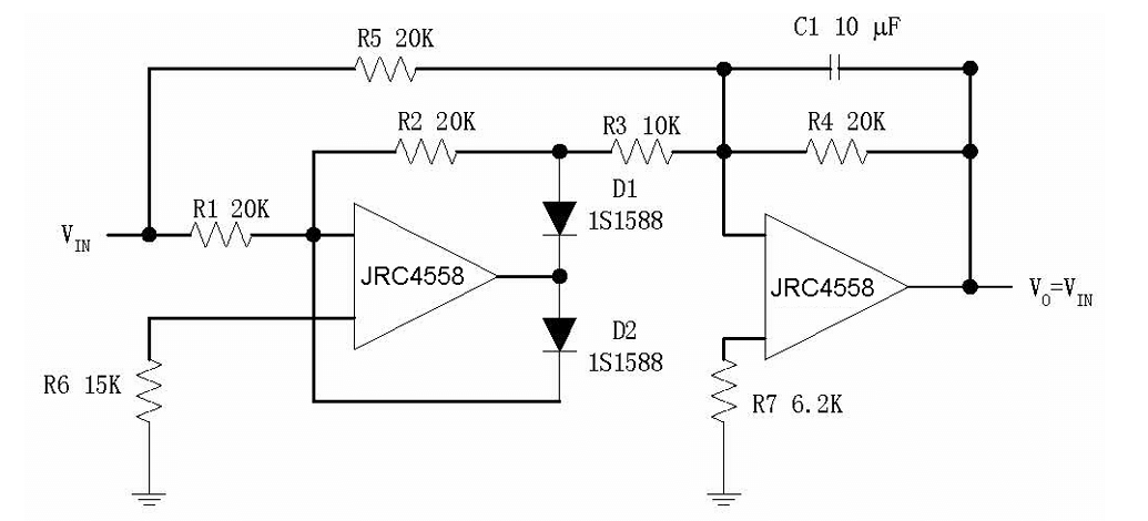
Figure 6: Input and Output Stage of the JRC4558
Output Stage of the JRC4558
The output stage of the JRC4558 is designed to deliver a strong, clear signal to the load with minimal energy loss. It uses a Class AB push-pull emitter follower configuration that provides high current gain while maintaining efficiency. A Vbe Multiplier is employed to set the bias current, ensuring the amplifier operates correctly at rest and responds quickly to dynamic changes.
Components including transistors Q11 and Q12, and resistors R6, R7, and R8, work to ensure the amplifier can drive different types of loads reliably. Ballast resistors are included to improve thermal stability and distribute current evenly that helps maintain performance and prolongs the life of the amplifier. This careful design makes the JRC4558 well-suited for demanding applications that require both accuracy and durability.
JRC4558 vs. TL072
Figure 7: JRC4558 vs. TL072
The JRC4558 and TL072 are both dual operational amplifiers but they have some differences that affect how they perform in circuits. The JRC4558 is simple and works well in basic dual op-amp setups, and a common choice for small and efficient circuits. On the other hand, the TL072 is designed for more complex circuits. It has a better internal structure that helps with signal quality and stability, that is important for circuits that need precise signal handling.
The TL072 works well with a wide variety of voltages and produces very little noise, great for amplifying audio signals without losing quality. It is also power-efficient and can handle quick signal changes without issues like latch-ups or short circuits, and reliable choice for systems that need high precision.
The TL072 is versatile and can be used in many different circuits, from audio pre-amps to solar power systems. It's also reliable in devices like uninterruptible power supplies (UPS) and oscilloscopes, showing its adaptability for both audio processing and power management tasks.
Other operational amplifiers similar to the TL072 include the LM358, NE5532, OPA827, LT1972, and ADA4610-2. Each has its own strengths, so designers can choose one that fits their specific needs and budget.
JRC4558 vs. NE5532
The JRC4558 is great for simple applications. In contrast, the NE5532 is designed for high-performance applications like professional audio, where minimizing noise and distortion is important for achieving clear sound quality.
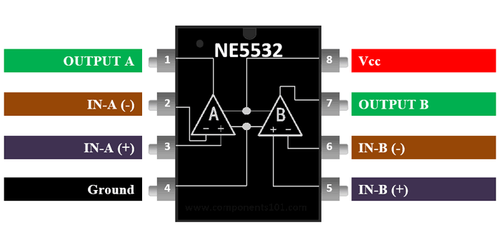
Figure 8: NE5532 Pinout
The NE5532 is excellent for audio work because it has low noise and a wide bandwidth. Its high common-mode rejection ratio and strong voltage gain allow it to amplify weak signals. It also handles a wide range of input signals and processes them quickly and accurately.
The NE5532 used in audio devices like pre-amplifiers, tone controls, and graphic equalizers, as well as professional audio mixing consoles. It's a top choice for audio professionals who need reliable, high-quality sound performance.
Alternatives to the NE5532 include the TL072, TL1971, LM358, LM4558, RC4588, NJM4560, and LM258. Each of these has different strengths, allowing for a range of options depending on the project's needs.
JRC4558 Packages Options
DIP-8 (Dual In-line Package)
The DIP-8 package is known for its straightforward parallel pin arrangement, and ideal for breadboarding and quick prototyping. The larger size of this package allows easy insertion into standard sockets or through-hole soldering on printed circuit boards (PCBs).
This package is favored in projects where manual adjustments or component replacements are expected. Commonly used in educational kits, DIY electronics, and even some commercial products, DIP-8 provides a user-friendly experience for assembling and troubleshooting circuits. The spacing between pins and the physical size of the package make it suited for manual handling and debugging.
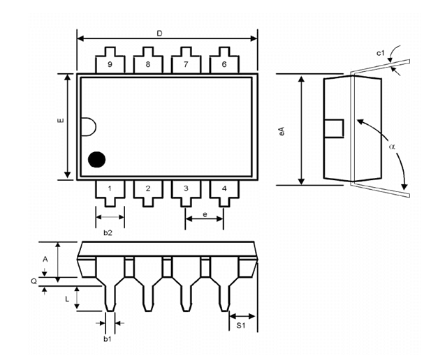
Figure 9: DIP-8 Package
|
SYMBOL |
INCHES |
MILLIMETERS |
||
|
MIN |
MAX |
MIN |
MAX |
|
|
A |
- |
0.2 |
- |
5.08 |
|
b1 |
0.014 |
0.023 |
0.36 |
0.58 |
|
b2 |
0.045 |
0.065 |
1.14 |
1.65 |
|
c1 |
0.008 |
0.015 |
0.2 |
0.38 |
|
D |
0.355 |
0.4 |
9.02 |
10.16 |
|
E |
0.22 |
0.31 |
5.59 |
7.87 |
|
e |
0.100 BSC |
2.54 BSC |
||
|
eA |
0.300 BSC |
7.62 BSC |
||
|
L |
0.125 |
0.2 |
3.18 |
5.08 |
|
Q |
0.015 |
0.06 |
0.38 |
1.52 |
|
s1 |
0.005 |
- |
0.13 |
- |
|
α |
90° |
105° |
90° |
105° |
SOP-8 (Small Outline Package)
The SOP-8 package is a more compact design intended for surface-mount technology (SMT). Its smaller size allows for greater component density on PCBs, making it an excellent choice for modern electronics where space is limited.
This package is optimized for automated assembly, ensuring more efficient production lines and reliable mechanical mounting. Due to its lower profile and reduced footprint, SOP-8 is used in portable devices or applications with strict space constraints. It supports scalable production processes and well-suited for high-volume manufacturing.
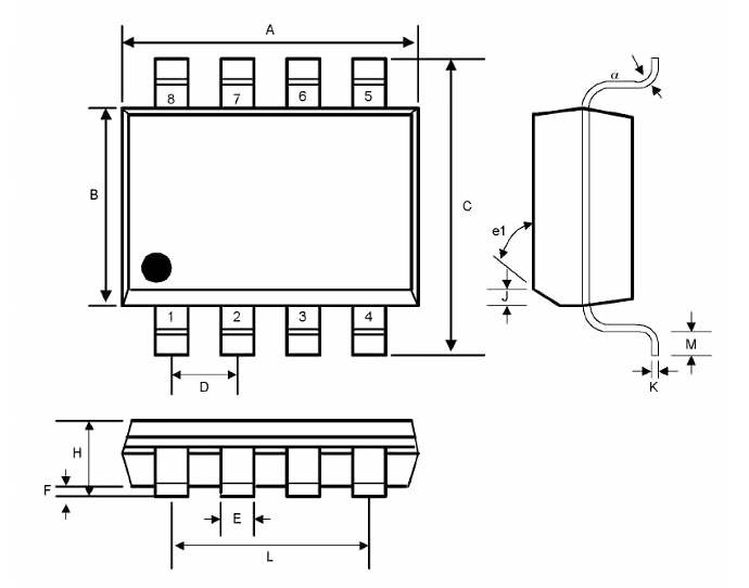
Figure 10: SOP-8 Package
|
Symbol |
INCHES |
MILLIMETERS |
||
|
MIN |
MAX |
MIN |
MAX |
|
|
A |
0.188 |
0.197 |
4.8 |
5 |
|
B |
0.149 |
0.158 |
3.8 |
4 |
|
C |
0.228 |
0.244 |
5.8 |
6.2 |
|
D |
0.050 BSC |
1.27 BSC |
||
|
E |
0.013 |
0.02 |
0.33 |
0.51 |
|
F |
0.004 |
0.01 |
0.1 |
0.25 |
|
H |
0.053 |
0.069 |
1.35 |
1.75 |
|
J |
0.011 |
0.019 |
0.28 |
0.48 |
|
K |
0.007 |
0.01 |
0.19 |
0.25 |
|
M |
0.016 |
0.05 |
0.4 |
1.27 |
|
L |
0.150 REF |
3.81 REF |
||
|
e1 |
45° |
45° |
||
|
α |
0° |
8° |
0° |
8° |
Conclusion
The JRC4558 operational amplifier stands out for its stability, high performance, and versatility. With features like a wide voltage range, high voltage gain, and low-noise input, it's ideal for applications such as audio processing and precision instruments. The article compares it to alternatives like the TL072 and NE5532, offering valuable guidance for selecting components. Overall, the JRC4558 has played a major role in advancing electronic design.
Frequently Asked Questions [FAQ]
1. What is the bandwidth of JRC4558?
The JRC4558 IC, offers a bandwidth of 3 MHz. This bandwidth ensures the IC can handle audio signals without loss of fidelity and for tasks like audio amplification, and signal conditioning.
2. What is the supply voltage of JRC4558?
The JRC4558 operates within a dual supply voltage range of ±5V to ±18V. This flexibility in supply voltage allows it to be used in various electronic devices, from small battery-operated units to larger, mains-powered equipment.
3. What is the maximum voltage for 4558 IC?
The maximum voltage for the 4558 IC is ±18V. Applying a voltage higher than this can lead to overheating and potentially permanent damage to the IC, so it’s required to ensure the voltage stays within this limit during operations.
4. What is IC 4558 used for?
The IC 4558 is used in audio signal processing. Its applications include being a main component in audio pre-amplifiers, mixers, and active filters. This IC is favored for these applications due to its low noise output and the ability to operate over a wide range of voltages, accommodating various audio equipment needs.
5. What is the slew rate of 4558?
The slew rate of the JRC4558 is 1 V/µs. This rate determines how quickly the output of the IC can respond to a rapid change in the input signal. A slew rate of 1 V/µs is adequate for handling most audio applications, preventing signal distortion during rapid changes in the input audio signal.