ADC0809 vs. ADC0832: Key Differences in 8-Bit AD Converters
Catalog
ADC0809 Overview
ADC0809 is an 8-channel, 8-bit successive approximation A/D analog-to-digital converter using CMOS technology. It integrates an 8-channel multiplexer inside, which can latch the decoded signal according to the address code and select only one of the 8 analog input signals for A/D conversion. ADC0809 is mainly suitable for occasions that do not require high accuracy and sampling rate, such as general industrial control fields. It can be directly connected to the microcontroller to achieve data conversion and transmission.
Characteristics of ADC0809
It has the following characteristics:
• Typical conversion speed 100us
• Unipolar, range 0-5V
• Successive approximation 8-bit A/D conversion chip
• There is a three-state output buffer on-chip, which can be directly connected to the CPU bus.
• There are 8 analog switches on the chip, which can connect 8 analog quantities at the same time.
• It has a high performance-price ratio and is suitable for occasions with low requirements on accuracy and sampling speed or in general industrial control fields.
Pin Description of ADC0809
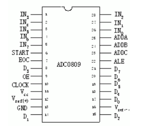
• D0~D7: 8-bit digital output pin
• IN0~IN7: 8 analog input pins
• Vcc: +5V working power supply
• GND: Ground
• VREF(+): Positive terminal of reference voltage
• VREF(-): Negative terminal of reference voltage
• START: A/D conversion start signal input terminal
• ALE: Address latch enable signal input terminal
• EOC: End of conversion output pin
• OE: Output enable control terminal
• CLK: Conversion clock signal, about 500kHz
• ADDA, ADDB, ADDC: Address input lines
How to Use ADC0809
The following is how to use the ADC0809.
Set the Analog Channel Input
We need to select through the three pins ADDA, ADDB, and ADDC. These three pins together form the input port of the analog channel selection address signal. The status of these pins determines which analog signal the ADC0809 will select for subsequent A/D conversion.
Start A/D Conversion
We need to select through three pins ADDA, ADDB, and ADDC. These three pins together form the input port of the analog channel selection address signal. The status of these pins determines which analog signal the ADC0809 will select for subsequent A/D conversion.
Determine Whether the A/D Conversion Is Completed
After the conversion is started, the EOC (end of conversion signal) will automatically convert from high level to low level. During A/D conversion, EOC remains low. After the conversion is completed, the EOC will automatically change from low to high. Therefore, we can judge whether the A/D conversion is completed by judging the value of EOC.
Output the Converted Data
When OE is high level, ADC0809 will allow the output of the data converted by A/D. At this time, the converted digital signal will be transmitted to the output port of the ADC0809 for reading or use by external devices.
Function and Use of ADC0809
The main function of ADC0809 is to convert analog input signals into digital output signals, which has the characteristics of high accuracy, fast conversion, and ease of use. It can be widely used in many fields, such as medical equipment, power monitoring, military equipment, communication electronics, aerospace, and industrial automation control. The following lists some typical application scenarios:
Medical Equipment
ADC0809 can be used to monitor and process physiological parameters (such as blood pressure, heart rate, etc.) in medical devices to meet the accuracy and stability requirements of medical equipment. For example, in digital sphygmomanometers, electrocardiographs, and other equipment, ADC0809 can collect and process physiological parameters, and convert them into digital signals for analysis and display, thereby achieving effective monitoring and diagnosis of patient conditions.
Communication Electronics
ADC0809 can be used to realize digital conversion and processing of analog signals to meet the requirements of communication electronic equipment for signal quality and transmission speed. For example, in audio processors, modems, voice codecs, and other equipment, ADC0809 can collect and process analog signals and convert them into digital signals for transmission and processing, thereby achieving efficient processing and transmission of communication signals.
Power Monitoring
ADC0809 can be used to monitor parameters such as power quality, grid load, and voltage stability to achieve real-time monitoring and management of the operating status of the power system. For example, in power monitoring instruments, smart meters, and other equipment, ADC0809 can collect and process circuit parameters, and convert them into digital signals for transmission and storage, thereby achieving effective monitoring and management of the power system.
Industrial Automation Control
ADC0809 can be used to monitor various industrial parameters such as voltage, pressure, temperature, flow, etc. to achieve monitoring and control of the production process. For example, in frequency converters, liquid level gauges, gas detectors, and other equipment, ADC0809 can collect and process analog data, and convert it into digital signals for analysis and feedback, thereby achieving effective control of the production process.
Internal Structure and Working Process of ADC0809
ADC0809 is a CMOS monolithic successive approximation A/D converter. It consists of 8 analog switches, successive approximation registers, comparators, 8-bit switch tree A/D converters, address latches and decoders, and logic control and timing circuit.
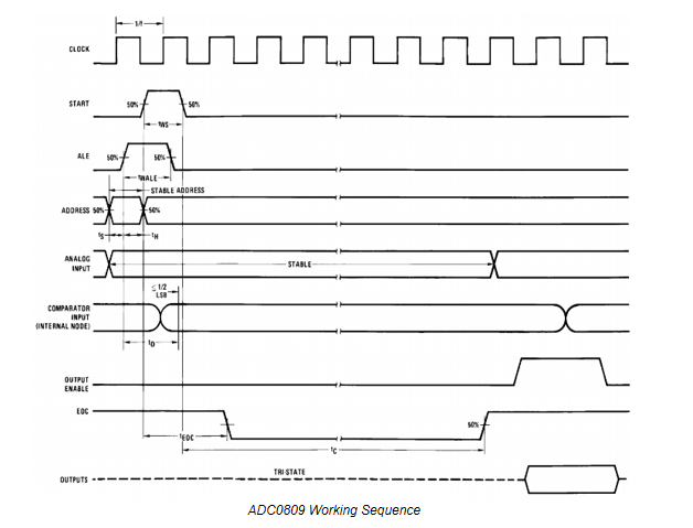
First, you need to enter a 3-bit address and set ALE to 1 to store this address in the address latch. This address is then passed through a decoder, which selects one of the eight analog inputs and feeds it to the comparator. When the rising edge of the START signal arrives, the successive approximation register will be reset. Subsequently, the falling edge of the START signal will start the A/D conversion process. When the A/D conversion starts, the EOC output signal will go low to indicate that the conversion is in progress. When the A/D conversion is completed, the EOC output signal will change to high level, which indicates that the A/D conversion has ended and the result data has been stored in the latch. The EOC signal can be used as an interrupt request to notify external devices (such as microcontrollers) that the conversion has been completed. When the OE (Output Enable) input is high, the output tri-state gate will be opened so that the digital quantity of the conversion result can be output to the data bus. The data obtained after A/D conversion should be transmitted to the microcontroller in time for processing to ensure the real-time and accuracy of the data. The key issue in data transmission is how to confirm the completion of A/D conversion, because transmission can only be carried out after confirmation is completed. There are three ways to do this.
Timing Transmission Method
For A/D converters, conversion time is a known and fixed specification. Taking ADC0809 as an example, its conversion time is 128μs. In a 6MHz MCS-51 microcontroller system, this is equivalent to 64 machine cycles. Based on this information, we can design a delay subroutine that is called immediately after the A/D conversion is started. The execution time of the delay subroutine should ensure that it ends when the conversion is completed, and then the data transfer can take place.
Query Method
A/D conversion chips usually have a status signal indicating completion of conversion. Taking ADC0809 as an example, this signal is the EOC terminal. Therefore, we can use the query method to confirm whether the A/D conversion has been completed by detecting the status of the EOC, and then proceed with data transmission after confirmation.
Interruption Mode
We use the status signal (EOC) indicating the completion of conversion as an interrupt request signal to transmit data in an interrupt manner.
How Does the Power Consumption of ADC0809 Affect Its Performance?
The impact of the power consumption of ADC0809 on its performance cannot be ignored, which is reflected in the following key aspects:
Heat Generation: Power consumption is directly related to the heat generated by the device. As power consumption increases, ADCO809 will generate more heat during operation. If the heat cannot be dissipated effectively, it may cause the internal temperature of the device to rise, affecting its stability and reliability. Excessive temperature may cause damage or performance degradation of circuit components, thereby affecting the conversion accuracy and speed of the ADC0809.
Power Management: The level of power consumption will also affect the design of the power management system. The low-power ADCO809 allows the use of smaller power supplies and reduces energy losses during power conversion. This is very important to improve the efficiency and reliability of the entire system.
Energy Consumption Efficiency: The level of power consumption directly affects the energy consumption efficiency of the device. Low-power devices save energy and reduce environmental impact when running for long periods of time. This is especially important for portable devices or systems that need to run for long periods of time.
Heat Dissipation Design: In order to ensure that the device can work stably, it requires a reasonable heat dissipation design to ensure that the heat can be effectively dissipated. This may involve the use of radiators, fans, or other cooling measures.
The Difference Between ADC0809 and ADC0832
ADC0809 and ADC0832 are two common 8-bit analog-to-digital converters (ADCs). The differences between them are as follows:
Sampling Rate: There is a certain difference in the maximum sampling rate of ADC0809 and ADC0832. The ADC0809 has a maximum sampling rate of 10kHz, while the ADC0832 has a maximum sampling rate of 100kHz.
Frequently Asked Questions [FAQ]
1. What is ADC0809?
The ADC0809 data acquisition component is a monolithic CMOS device with an 8-bit analog-to-digital converter, 8-channel multiplexer and microprocessor compatible control logic. The 8-bit A/D converter uses successive approximation as the conversion technique.
2. What is the role of ADC0809 in PCM?
The ADC0809 includes 8 analog inputs due to the 8-channel multiplexer circuit. Since the resolution of ADC0809 is 8 bits, the analog input is divided into 28 , or 256 discrete ranges. With 5Vdc reference voltage, each range represents 5V/256=0.01953 V.
3. How does an ADC 0808/0809 work?
The ADC 0808/0809 works by utilizing a process called successive approximation. It first samples the input analog signal and then compares it with a reference voltage. Based on this comparison, the ADC generates a digital output that represents the magnitude of the analog signal.
4. What is the difference between ADC 0808 and 0809?
These two converters, the ADC0808 and ADC0809, are functionally identical except that the ADC0808 has a total unadjusted error of ±1⁄2 LSB and the ADC0809 has an unadjusted error of ±1 LSB. They are also related to their big brothers, the ADC0816 and ADC0817 expandable 16 channel converters.