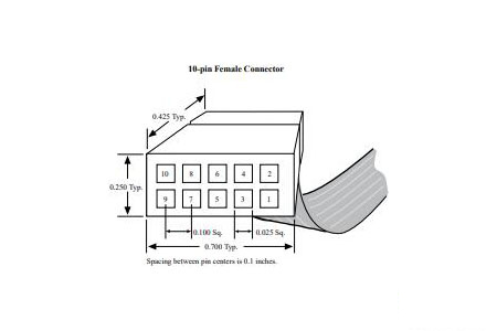
Pinout and Block Diagram of the PL-USB2-BLASTER Cable
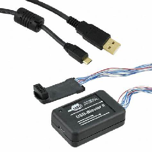
The PL-USB2-BLASTER is an important component of Intel's FPGA Download Cable series, enabling the configuration of Intel® FPGAs via a USB connection. This article provides a detailed look at its design and functionality, including its pinout, features, block diagram, connections, and operational specifics. We aim to explore not only the technical details of the device but also the ease and effectiveness it brings to FPGA configurations.Catalog
What is the PL-USB2-BLASTER?
The PL-USB2-BLASTER is a great component in the Intel® FPGA Download Cable series, facilitating efficient data transfer between a computer and an FPGA through a USB connection. This cable enhances iterative prototyping and production programming by conveying configuration data via a standard 10-pin header on a circuit board. Grasping the core functionalities of the PL-USB2-BLASTER is use for its effective deployment across different stages of FPGA development. This device ensures seamless integration in various development environments, characterized by its rapid and consistent data transmission capabilities.
During iterative prototyping stages, precision and agility are needed. The PL-USB2-BLASTER supports quick uploading of updated configurations, enabling rapid testing and adjustments of FPGA setups. This agility is beneficial in environments necessitating frequent iterations to fine-tune designs and promptly address issues. Consistency in performance is required in production programming. The PL-USB2-BLASTER guarantees accurate programming of final configurations into the FPGA, ensuring reliability in end-use applications. This consistency helps minimize discrepancies and enhances efficiency, particularly when programming large volumes of units.
Pinout of PL-USB2-BLASTER
|
Pin Number |
Pin Name |
Function Description |
|
1 |
DCL |
The DCL pin is good for propagating the clock signal
for synchronous operations. It is important to minimize noise and maintain
stable connections similar to high-frequency circuit design practices. |
|
2 |
GND |
Ground (GND) serves as the reference voltage, ensuring
consistent and reliable grounding to prevent discrepancies in signal levels
and mitigate issues such as ground loops. |
|
3 |
CONF_DONE |
The CONF_DONE pin indicates the completion of device
configuration. Monitoring this pin is use for verifying the successful
initialization of peripherals. |
|
4 |
Vocc (TRGT) |
The Vocc pin supplies power to the target system, with a
focus on delivering the correct voltage to avoid under or over-voltage
conditions, utilizing power management regulation methods. |
|
5 |
nCONFIG |
The nCONFIG pin facilitates device reconfiguration upon
activation, ensuring resetting or reprogramming is achieved without
interruptions. |
|
6 |
nCE |
The nCE (Chip Enable) pin controls the enabling state of
the device, requiring proper assertion to activate the device when necessary,
akin to controlling enable signals in integrated circuits. |
|
7 |
DATAOUT |
DATAOUT is responsible for the output of data, focusing
on clean signal transmission to safeguard data integrity and incorporate
error-checking protocols against data corruption. |
|
8 |
nCs |
The nCs (Chip Select) pin activates specific device
components, with controlled activation and deactivation to ensure the correct
parts of a device are engaged at the right times. |
|
9 |
ASDI |
ASDI is used for input data, emphasizing the need for
precise and timely data input, synchronizing input similar to sequential
logic circuits to prevent miscommunication. |
|
10 |
GND |
Similar to Pin 2, Pin 10 provides another grounding
point, focusing on implementing multiple grounding points as a strategy
common in high-precision systems to enhance stability and performance. |
PL-USB2-BLASTER Functional Diagram
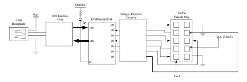
Data Routing and Communication Pathways
The host computer interface serves as the initial point of contact for configuration data. Acting as a conduit between the computer’s software and the PL-USB2-BLASTER hardware, this interface harnesses high-speed USB 2.0 protocols to facilitate rapid and reliable data transmission. Following data reception, the processing unit within the PL-USB2-BLASTER assumes control. This unit, comprising either a microcontroller or FPGA, diligently parses, checks for errors, and formats incoming data to ensure compatibility with subsequent components.
Post-processing, data is temporarily housed in buffering units. These buffers handle timing discrepancies between high-speed data influx and varying downstream processing speeds. Effective buffer management practices are needed, as they reduce interruptions and data loss. The next step involves transmitting the buffered data to the FPGA through a clearly defined routing network. This network, involving multiplexers, demultiplexers, and dedicated pathways, is crafted to preserve data integrity and synchronization. A well-implemented routing network is important; suboptimal routing can lead to configuration errors and performance issues, as noted in many practical applications.
Synchronization and Timing Control
A cornerstone of the architecture is the clock generation and distribution system, which orchestrates data transfer timing to ensure seamless operation. Precision in clock distribution is often highlighted by others as use for maintaining synchronization and optimal performance. Maintaining signal integrity is also a key component of the PL-USB2-BLASTER's architecture. Techniques such as differential signaling, impedance matching, and shielded pathways are employed to mitigate signal degradation and electromagnetic interference (EMI).
Advanced Configuration Mechanisms
The architecture diagram also depicts mechanisms for error detection and correction. Techniques such as cyclic redundancy checks (CRC) and other error-detection algorithms automatically identify and correct data stream discrepancies, ensuring the reliability of the configuration process. These methods are highly valued in numerous applications for their role in establishing robust systems. Dynamic reconfiguration capabilities represent another sophisticated feature of the PL-USB2-BLASTER. This functionality allows for FPGA configuration modifications without halting operations, a trait immensely valued in scenarios where adaptability and minimal downtime are required.
Using PL-USB2-BLASTER
Driver Installation
Kick off the process by downloading and installing Intel's provided drivers. These drivers serve as a bridge for communication between the cable and your computing device. You will find comprehensive instructions in the driver package, offering a step-by-step guide through the installation.
Hardware Connection
After installing the drivers, link the PL-USB2-BLASTER cable from your computer’s USB port to the target device's programming port. This connection is good for preparing the hardware components for the forthcoming configuration.
Launching Quartus Prime Programmer
Fire up the Intel Quartus Prime software, head over to the 'Programmer' tool, and pick the fitting hardware configuration file. The software’s friendly interface ensures a simple setup process, enabling swift adjustments and configurations.
Performing Device Configuration
Deploy the Quartus Prime Programmer to execute device configuration. Choose the target device from the list and upload the relevant project files. Initiate the programming sequence, and the software will manage the data transfer, effectively configuring your FPGA device.
Signal Tap's Role
The PL-USB2-BLASTER cable extends support to the Signal Tap Logic Analyzer, a tool for rigorous logical analysis. Signal Tap offers embedded logic analysis, a feature for debugging and verifying FPGA designs.
Setting Up Signal Tap
Within the Quartus Prime software, configure the Signal Tap Logic Analyzer to capture and scrutinize signals. By defining specific trigger conditions, you can meticulously control data collection, aiding in pinpointing issues within the FPGA design.
The adept use of the PL-USB2-BLASTER cable demands a profound grasp of both hardware and software realms. Integrating these tools into the design process can notably streamline development cycles and enhance the final product's reliability. The merging of thorough setup and analytical capabilities truly augments the effectiveness of FPGA development. Adhering to these guidelines and leveraging the comprehensive features of the PL-USB2-BLASTER cable and Quartus Prime software enable to craft a robust and efficient development workflow, ensuring superior performance and reliability of their FPGA designs.
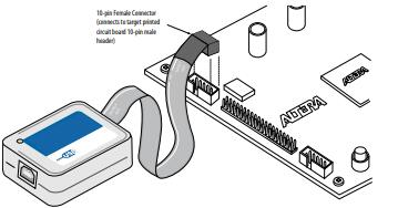
Cable-to-Board Connection
Safety Measures for Secure Operation
First and foremost, make sure to disconnect all power sources before starting the cable-to-board connection. This precaution shields against electrical hazards and safeguards the delicate components on the device board.
Establishing the Connection
Begin by attaching the Intel FPGA Download Cable to the PC. Proceed to connect the cable to the 10-pin header on the device board. After verifying that all connections are secure, restore the power supply. Secure connections can avert data errors and facilitate strong communication pathways between devices.
Installing the Driver
If the system signals the need for new hardware driver installation, exit the initial wizard. Adhering to the manufacturer's installation guidelines ensures that the appropriate drivers are properly installed. This approach nurtures the device's optimal performance capabilities. Careful adherence to Intel's step-by-step installation instructions can prevent incomplete installations that may result in system glitches.
Detaching the Cable
Remove the power supply before unplugging the cable to prevent any potential electrical damage. Proceed by unplugging the cable from the device board, followed by disconnecting it from the PC. The proper disconnection sequence can mitigate risks tied to sudden power surges. Following a systematic disconnection process supports the longevity of hardware components and can curtail repair expenses.
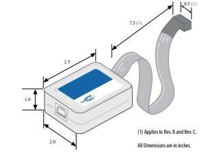
PL-USB2-BLASTER Dimensions
Frequently Asked Questions [FAQ]
1. What is the purpose of a USB Blaster?
A USB Blaster enables PC users to program and configure in-system devices via a USB connection. This tool streamlines the development process for you, making it a reliable companion in their creative and technical pursuits.
2. How does the USB Blaster differ from the USB Blaster II?
The USB Blaster I supports JTAG circuits between 2.5V and 3.3V. In contrast, the USB Blaster II caters to a broader voltage range from 1.5V to 5V and offers advanced features. The versatility of the USB Blaster II allows for compatibility with a wider variety of systems, expanding its usability. This adaptability enhances its functionality, making it a highly sought-after tool in more complex scenarios.
3. What are the steps to install a USB-Blaster driver?
Firstly, connect the USB-Blaster to your PC. Upon connection, follow the on-screen prompts to choose driver installation options. Navigate to the drivers located in the Quartus Prime installation directory and proceed with the installation wizard until the process is fully completed. This straightforward method ensures seamless integration with your development environment. The ease of this process allows you to focus more on innovation and creativity.
4. What prerequisites are necessary for using the Intel FPGA Download Cable?
Commence by installing the appropriate drivers on your system. This initial step is important. Subsequently, configure the hardware via the Intel Quartus® Prime software. This preparation fine-tunes your setup for optimal performance and efficiency.
5. What does Intel recommend for optimal use of the Intel FPGA Download Cable?
Intel strongly advises using the most recent version of Quartus Prime software. By staying updated with the latest iterations, others gain access to enhanced features and improved performance. This practice ensures a more streamlined and making each interaction with the tool more productive.