PCF8591 A/D and D/A Converter Datasheet and Raspberry Pi Integration
The PCF8591 is a versatile 8-bit CMOS data acquisition chip renowned for its low power usage and convenient integration through an I2C-bus interface. With four analog inputs and a single analog output, it is ideal for applications that effectively handle multiple analog signals, such as environmental monitoring or smart home systems. This article provides a comprehensive look at the PCF8591's features, practical uses, and integration with platforms like the Raspberry Pi. Through its 8-bit resolution, the PCF8591 ensures accurate data conversion, making it a popular choice for both educational projects and professional IoT setups where precision and efficiency are used.Catalog
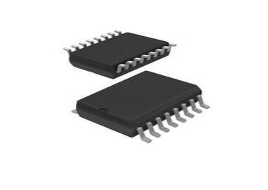
Pin Configuration
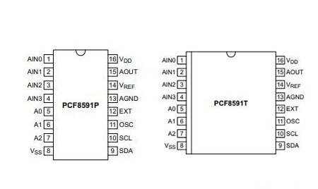
|
Pin Number |
Pin Name |
Description |
|
1 |
AINO |
Analogue inputs (AD converter) |
|
2 |
AIN1 |
Analogue input 1 |
|
3 |
AIN2 |
Analogue input 2 |
|
4 |
AIN3 |
Analogue input 3 |
|
5 |
A0 |
Hardware slave address |
|
6 |
A1 |
Hardware slave address |
|
7 |
A2 |
Hardware slave address |
|
8 |
Vss |
Ground supply voltage |
|
9 |
SDA |
I2C-bus serial data input and output |
|
10 |
SCL |
I2C-bus serial clock input |
|
11 |
OSC. |
Oscillator input/output |
|
12 |
EXT |
External/internal switch for oscillator input |
|
13 |
AGND |
Analogue ground supply |
|
14 |
VREF |
Voltage reference input |
|
15 |
AOUT |
Analogue output (D/A converter) |
|
16 |
Voo |
Supply voltage |
Overview of PCF8591
The PCF8591 offers a dynamic approach with its single-supply 8-bit A/D and D/A conversion capabilities, equipped with the I2C interface. This setup allows for a streamlined digital-analog system design, making it mostly appealing in settings with limited resources. By supporting both analog input and output via a common interface, it facilitates effective data management and control within embedded systems.
Address pins (A0, A1, A2) significantly enhance its application by permitting up to eight devices on a single I2C bus. This feature proves advantageous in complex systems that integrate multiple sensors, reducing wiring needs and easing installations. Effective address handling enables refined data flow and device distribution, minimizing potential failures. The I2C interface promotes streamlined serial data communication, simplifying transfer processes and improving coordination across devices.
CAD Representations
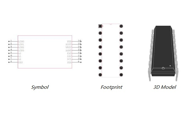
CAD Model for PCF8591P
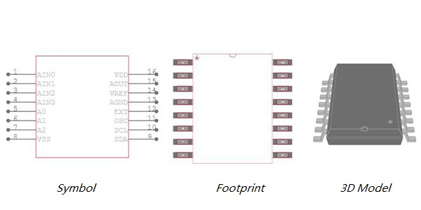
CAD Models for PCF8591T
Technical Specifications
This table captures the essential specifications, attributes, and parameters for the NXP USA Inc. PCF8591T/2,518, including relevant compliance and packaging details.
|
Type |
Parameter |
|
Factory Lead Time |
7 Weeks |
|
Mounting Type |
Surface Mount |
|
Package / Case |
16-SOIC (0.295, 7.50mm Width) |
|
Surface Mount |
YES |
|
Operating Temperature |
-40°C to 85°C |
|
Packaging |
Tape & Reel (TR) |
|
Published |
1997 |
|
JESD-609 Code |
e4 |
|
Part Status |
Active |
|
Moisture Sensitivity Level (MSL) |
3 (168 Hours) |
|
Number of Terminations |
16 |
|
Type |
ADC, DAC |
|
Terminal Finish |
Nickel/Palladium/Gold (Ni/Pd/Au) |
|
Voltage - Supply |
2.5V to 6V |
|
Terminal Position |
DUAL |
|
Terminal Form |
GULL WING |
|
Peak Reflow Temperature (°C) |
260 |
|
Number of Functions |
1 |
|
Supply Voltage |
5V |
|
Terminal Pitch |
1.27mm |
|
Time@Peak Reflow Temperature-Max (s) |
40 |
|
Base Part Number |
PCF8591 |
|
Pin Count |
16 |
|
JESD-30 Code |
R-PDSO-G16 |
|
Qualification Status |
Not Qualified |
|
Supply Voltage-Max (Vsup) |
6V |
|
Supply Voltage-Min (Vsup) |
2.5V |
|
Number of Channels |
4 |
|
Data Interface |
I2C, Serial |
|
Sampling Rate (Per Second) |
11.1k |
|
Voltage Supply Source |
Single Supply |
|
Resolution (Bits) |
8 bits |
|
Length |
10.3mm |
|
Height Seated (Max) |
2.65mm |
|
Width |
7.5mm |
|
RoHS Status |
ROHS3 Compliant |
Comparable Parts
|
Part Number |
Manufacturer |
Package / Case |
Supply Voltage |
Brand Name |
Terminal Pitch |
Factory Lead Time |
Peak Reflow Temperature (°C) |
Terminal Position |
Number of Terminations |
View Compare |
|
PCF8591T/2,518 |
NXP USA Inc. |
16-SOIC (0.295, 7.50mm Width) |
5 V |
NXP Semiconductor |
1.27 mm |
7 Weeks |
260 |
DUAL |
16 |
PCF8591T/2,518 VS PCA9546AD,118 |
|
PCA9546AD,118 |
NXP USA Inc. |
16-SOIC (0.154, 3.90mm Width) |
3.3 V |
NXP Semiconductor |
1.27 mm |
7 Weeks |
260 |
DUAL |
16 |
PCF8591T/2,518 VS PCA9546AD,118 |
|
PCA9554D,112 |
NXP USA Inc. |
16-SOIC (0.295, 7.50mm Width) |
3 V |
NXP Semiconductor |
1.27 mm |
7 Weeks |
260 |
DUAL |
16 |
PCF8591T/2,518 VS PCA9554D,112 |
|
PCA9672D,512 |
NXP USA Inc. |
16-SOIC (0.295, 7.50mm Width) |
3 V |
NXP Semiconductor |
1.27 mm |
7 Weeks |
260 |
DUAL |
16 |
PCF8591T/2,518 VS PCA9672D,512 |
Features
|
Feature |
Description |
|
Power Supply |
Single power supply |
|
Operating Supply Voltage |
2.5 V to 6.0 V |
|
Standby Current |
Low standby current |
|
Serial Communication |
Serial input and output via I2C-bus |
|
I2C Address Selection |
Configurable by 3 hardware address pins |
|
Sampling Rate |
Determined by I2C-bus speed |
|
Analogue Inputs |
4 analogue inputs, configurable as single-ended or
differential |
|
Channel Selection |
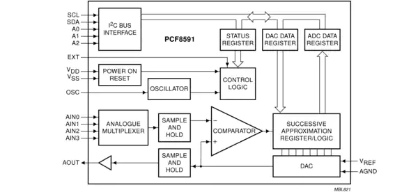
Auto-incremented channel selection |
|
Analogue Voltage Range |
From VSS to VDD |
|
Track and Hold Circuit |
On-chip track and hold circuit |
|
A/D Conversion |
8-bit successive approximation A/D conversion |
|
DAC |
Multiplying DAC with one analogue output |
Block Diagram
Uses of the PCF8591
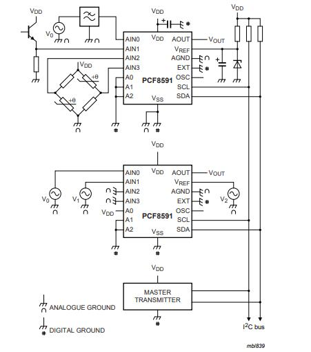
The PCF8591 is a versatile converter handling both analog-to-digital and digital-to-analog tasks. It seamlessly integrates with many systems, adeptly managing supply monitoring, setting precise references, and overseeing analog loops. Its adaptable nature allows it to blend into dynamic environments, enhancing complex system solutions.
Supply Monitoring
In monitoring supplies, the PCF8591 offers precise voltage and current readings. This level of accuracy supports systems demanding data, ensuring stability and performance. Consider a renewable energy scenario, solar panel outputs monitored by this device maintain peak function, demonstrating reliability across evolving situations.
Establishing References in Varied Applications
The art of setting references with the PCF8591 shines in areas like automated lighting. By modifying analog inputs, it adjusts sensor thresholds, encouraging energy conservation. Precision in calibration enhances adaptability and ensures sustainable operations.
Stability in Managing Analog Loops
In the world of analog loop management, the PCF8591 performs consistently by perpetually adjusting signal paths. Its utility is evident in industrial automation, where stable feedback loops are used for process control. Such dependability sparks innovation, facilitating systems to meet diverse operational demands.
Versatility in Multiple Environments
The adaptability of the PCF8591 is seen across differing environments, be it academic experiments or consumer electronics. Its smooth integration highlights a key role in advancing robustness and promotes exploration and adaptation in modern tech arenas.
Application Diagram
Internal Circuit
Interfacing PCF8591 with Raspberry Pi
Connecting the PCF8591 to a Raspberry Pi involves the activation of I2C and configuring pins with precision. Begin by enabling I2C on the Raspberry Pi through command-line tools. Establish a connection by linking the SDA and SCL pins of the PCF8591 with those on the Raspberry Pi, creating an efficient pathway for communication.
Raspberry Pi I2C Configuration
To enable I2C on the Raspberry Pi, utilize the raspi-configuration utility. Access the interface options and perform a system reboot to prepare the setup for I2C functionality. This preparation allows the Raspberry Pi to effectively engage with other I2C devices.
Identifying I2C Address on Raspberry Pi
After establishing the connection, determine the I2C address of the PCF8591 with specific terminal commands. This step enhances the reliability of communication between the Raspberry Pi and the PCF8591. In scenarios, precise address detection assists in optimizing data collection processes.
Package
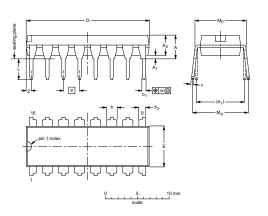
DIP16 Configuration
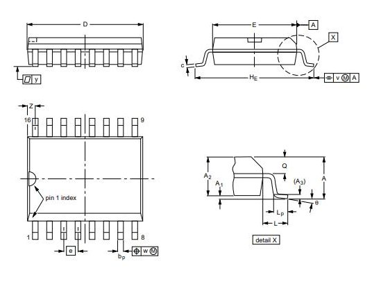
SO16 Configuration
Product Manufacturer
NXP Semiconductors, well-regarded for its secure connectivity solutions, has significantly influenced the evolution of embedded applications worldwide. With a rich history of innovation, the company has developed components known for their reliability and adaptability, enhancing technological integration and fostering new advancements.
The PCF8591 emerged to fulfill niche requirements within embedded systems, primarily as a device for converting between analog and digital signals. This component transforms signals into digital data, which is active for applications that demand precise sensor data interpretation. It thrives in settings where flexibility and data processing shape performance and guide decision-making.
Datasheet PDF
PCA9546AD,118 Datasheets:
Cylindrical Battery Holders.pdf
Frequently Asked Questions [FAQ]
1. What is PCF8591?
The PCF8591 serves as an 8-bit data acquisition tool harnessing I2C communication to facilitate seamless analog-to-digital and digital-to-analog transitions. This integration eases the complexity of operations within embedded systems. Its adaptability shines in tasks requiring precise data analysis and interpretation, simulating the exact challenges.
2. What is the function of PCF8591?
This device showcases multiplexing and track-and-hold features alongside strong A/D and D/A conversion capabilities. These attributes expand its reach into various applications such as environmental monitoring and interactive devices, representing diverse interests and interactions.
3. How do I connect my Raspberry Pi to PCF8591?
We dig into integrating the PCF8591 with a Raspberry Pi, emphasizing I2C interface configuration. This bond enriches the Raspberry Pi's capacity to communicate with analog sensors, key for projects dependent on data flow. Such setups cater to advancing automation efforts, similar to the ever-evolving pursuit of efficiency.
4. How does the pcf8591 work?
Through successive approximation conversion, the PCF8591 achieves precise signal measurement and generation. This reliable method is treasured in circles and industrial applications, echoing the quest for accuracy and dependability.
5. How many pcf8591s can be used on the same I2C bus?
Accommodating up to eight devices on a single I2C bus, this capability broadens input and output possibilities. Such scalability caters to intricate projects that challenge ingenuity, demanding a spectrum of data channels.
6. What is the DAC output on the pcf8591?
We explore constraints like the maximum output voltage linked to Vcc and related chip connections. Identifying these boundaries guides system design within safe margins, ensuring enduring functionality, akin to maintaining balance in endeavors.
7. What is a Raspberry Pi pcf8591 potentiometer?
Potentiometers function as variable resistors, with their analog output digitized for Raspberry Pi synergy. This interaction highlights the practical side of microcontroller projects, where sensor data morphs into actionable insights, echoing human decision-making.
8. How many 8-bit channels does the pcf8591 have?
Equipped with four 8-bit ADC channels and one DAC, the PCF8591 supports a variety of voltage measurement and generation tasks. Such versatility is ideal for environments enriched by multiple sensors, facilitating efficient signal management similar to mastering diverse skill sets.
9. What is the pcf8591 module?
Including the PCF8591 chip alongside passive elements for the analog signal interface, these components act as a bridge for analog and digital exchanges, fostering a streamlined design journey.
10. How do I connect the pcf8591 P3 to ain0?
By leveraging jumper caps to interface with P3, specific input configurations can be crafted, such as integrating a potentiometer on AIN0. This scenario illustrates flexibility and adaptability in circuit design, allowing for personalized solutions much like crafting unique personal experiences.
11. How do I measure the analog signal from the pcf8591?
A demonstration of using a potentiometer to gauge and produce genuine analog signals through PCF8591's capabilities. Mastery of this technique is used for advanced analog control systems, enhancing comprehension and performance, mirroring the drive for mastery and excellence.