Exploring LD1117S33TR PMIC Features and Datasheet Information
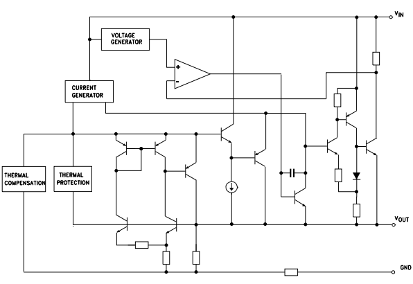
In the world of voltage regulation, the LD1117S33TR stands out as a reliable, low-dropout voltage regulator known for its adaptability and stability across various applications. Available in both adjustable and fixed configurations, it offers robust voltage management, maintaining a steady output even under fluctuating input conditions. With integrated thermal and short-circuit protections, the LD1117S33TR proves requisite in sensitive electronic environments, such as computer systems and communication devices. This article digs into its basic features, practical applications, and technical strengths, showcasing why you favor its straightforward yet effective design for creating compact, reliable power solutions.Catalog

Overview of the LD1117S33TR
The LD1117S33TR excels as a voltage regulator, offering up to 800 mA with an adjustable reference voltage beginning at 1.25 V. Its ease of integration into existing systems, thanks to pin-to-pin compatibility with standard industry modules, makes this device appealing for diverse applications.
The adjustable version of the LD1117S33TR provides noteworthy enhancements, such as lowering dropout voltage. This trait fosters efficient energy usage, ensuring systems remain stable amidst fluctuating input conditions. The enhanced voltage tolerance contributes to reliability, valued greatly in scenarios requiring a steady power supply. In practical application, the LD1117S33TR demonstrates versatility across numerous circuits. It garners appreciation for simplifying integration, thus reducing redesign costs and expediting development timelines.
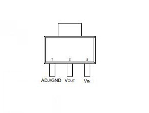
Pin Layout Details
|
Pin Number |
Pin Name |
Description |
|
1 |
Ground |
Ground Pin – connected to the ground of the system. |
|
2 |
Vout |
Regulated Output Voltage |
|
3 |
Vin |
Input Voltage that is to be regulated |
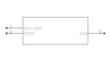
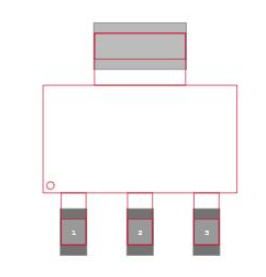
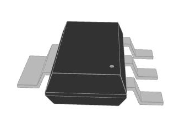
LD1117S33TR CAD Representation
Symbol
Footprint
3D Model
Alternatives
• LM1117MPX-3.3/NOPB
• LT1117IST-3.3#TR
• LD1117S30C
LD1117S33TR Applications
• Basic Configuration: To utilize a fixed voltage regulator version, you must connect the power source to the Vin pin and draw a stabilized output from the Vout pin, keeping the Adj/Ground pin grounded. Introducing a capacitor at the output can significantly reduce noise interference, which is principally beneficial in sensitive applications, ensuring clarity where noise might cause issues.
• Adjustable Output Configuration: For scenarios requiring adjustable output, connecting two resistors, R1 and R2, enables voltage tuning per the desired specification. Augmenting ripple rejection by adding a capacitor, CAdj, can enhance stability. You can often find that tweaking these components boosts performance, especially in dynamic environments demanding flexibility.
• Noise Management: Implementing additional capacitors at both the input and output offers effective noise filtration. This technique preserves signal integrity, an aspect active in precision electronics. Insights from field testing and iterative design improvements often guide optimal capacitor selection and placement, reflecting the depth of practical expertise.
Block Diagram
Application Circuit Design
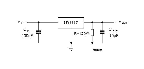
Circuit Configuration for 1.2 V Output
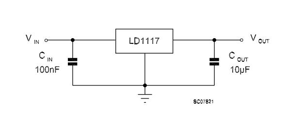
Crafting Circuits for Different Fixed Outputs
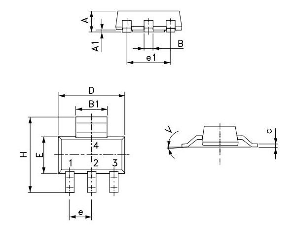
Dimensions
Technical Specifications
|
Type |
Parameter |
|
Lifecycle Status |
ACTIVE (Last Updated: 7 months ago) |
|
Factory Lead Time |
8 Weeks |
|
Contact Plating |
Tin |
|
Mount |
Surface Mount |
|
Mounting Type |
Surface Mount |
|
Package / Case |
TO-261-4, TO-261AA |
|
Number of Pins |
3 |
|
Weight |
4.535924g |
|
Operating Temperature |
0°C ~ 125°C |
|
Packaging |
Tape & Reel (TR) |
|
JESD-609 Code |
e3 |
|
Part Status |
Active |
|
Moisture Sensitivity Level (MSL) |
1 (Unlimited) |
|
Number of Terminations |
4 |
|
Termination |
SMD/SMT |
|
ECCN Code |
EAR99 |
|
Packing Method |
TR, 7 INCH |
|
Max Power Dissipation |
12W |
|
Terminal Position |
DUAL |
|
Terminal Form |
GULL WING |
|
Number of Functions |
1 |
|
Base Part Number |
LD1117 |
|
Pin Count |
4 |
|
JESD-30 Code |
R-PDSO-G4 |
|
Number of Outputs |
1 |
|
Output Voltage |
3.3V |
|
Output Type |
Fixed |
|
Max Output Current |
1.3A |
|
Voltage |
3.3V |
|
Max Supply Voltage |
15V |
|
Min Supply Voltage |
4.75V |
|
Output Configuration |
Positive |
|
Power Dissipation |
12W |
|
Quiescent Current |
10mA |
|
Accuracy |
1% |
|
Max Output Voltage |
3.3V |
|
Output Voltage 1 |
3.3V |
|
Number of Regulators |
1 |
|
Min Input Voltage |
4.75V |
|
Protection Features |
Over Current, Over Temperature |
|
Voltage Dropout (Max) |
1.2V @ 800mA |
|
PSRR |
75dB (120Hz) |
|
Dropout Voltage |
1.1V |
|
Nominal Input Voltage |
3.3V |
|
Dropout Voltage1-Nom |
1.1V |
|
Min Output Voltage |
3.3V |
|
Nominal Output Voltage |
3.3V |
|
Input Bias Current |
5mA |
|
Output Voltage Accuracy |
1% |
|
Height |
1.8mm |
|
Length |
6.5mm |
|
Width |
3.5mm |
|
REACH SVHC |
No SVHC |
|
Radiation Hardening |
No |
|
RoHS Status |
ROHS3 Compliant |
|
Lead Free |
Lead Free |
Comparable Parts
|
Part Number |
Manufacturer |
Package / Case |
Number of Pins |
Number of Outputs |
Max Output Current |
Min Input Voltage |
Nominal Input Voltage |
Min Output Voltage |
Nominal Output Voltage |
Output Voltage |
Max Output Voltage |
Accuracy |
View Compare |
|
LD1117S33TR |
STMicroelectronics |
TO-261-4, TO-261AA |
3 |
1 |
1.3 A |
4.75 V |
3.3 V |
3.3 V |
3.3 V |
3.3 V |
3.3 V |
1% |
LD1117S33TR VS NCP1117ST33T3G |
|
NCP1117ST33T3G |
ON Semiconductor |
TO-261-4, TO-261AA |
3 |
1 |
1.3 A |
3.6 V |
2.5 V |
2.5 V |
2.5 V |
2.5 V |
2.5 V |
1% |
LD1117S33TR VS NCP1117ST33T3G |
|
LD1117STR |
STMicroelectronics |
TO-261-4, TO-261AA |
4 |
1 |
1:00 AM |
3.5 V |
- |
3.3 V |
3.3 V |
3.3 V |
3.3 V |
1% |
LD1117S33TR VS LD1117STR |
|
LD1117S50CTR |
STMicroelectronics |
TO-261-4, TO-261AA |
3 |
1 |
1.3 A |
2.35 V |
- |
1.25 V |
- |
15 V |
15 V |
1% |
LD1117S33TR VS LD1117S50CTR |
|
LD1117S25TR |
STMicroelectronics |
TO-261-4, TO-261AA |
3 |
1 |
1.3 A |
6.5 V |
- |
5 V |
- |
5 V |
5 V |
1% |
LD1117S33TR VS LD1117S25TR |
Datasheet PDF
LD1117S33TR Datasheets:
NCP1117ST33T3G Datasheets:
Cylindrical Battery Holders.pdf
LD1117STR Datasheets:
LD1117S50CTR Datasheets:
LD1117S25TR Datasheets:
Frequently Asked Questions [FAQ]
1. What is LD1117S33TR?
The LD1117S33TR is a versatile low-dropout voltage regulator that can handle up to 800 mA of output current. Available in fixed and adjustable voltage versions, it offers multiple standard output voltages. Its widespread use is a testament to its efficiency and the flexible role it plays in delivering stable power supplies, especially in power-sensitive environments. The regulator showcases adaptability, meeting various technological requirements. In applications, you can find that the LD1117S33TR excels in heat-sensitive scenarios, helping extend device life and efficiency.
2. What is voltage dropout?
Voltage dropout is the smallest voltage difference needed between the input and output to ensure the regulator maintains the correct output voltage regulation. This measure reflects a regulator's efficiency, mostly when the input voltage nears the output voltage. A lower dropout voltage implies greater efficiency, which has remarkable implications for devices relying on limited power sources like batteries. In practice, reducing the dropout voltage can greatly enhance the longevity and performance of portable electronics by minimizing unnecessary power dissipation.