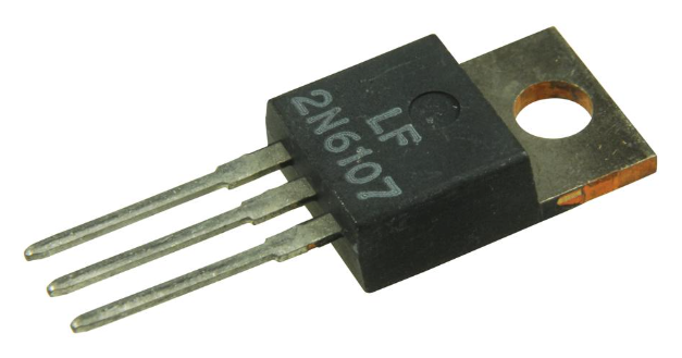
A Guide to Using the 2N6107 PNP Transistor in Electronics
This article explores the 2N6107, a versatile PNP transistor known for its efficiency in signal amplification and power switching applications. With a gain range between 30 and 150, this component finds itself at the heart of various electronic designs, from audio amplification to high-current management. We’ll look closer at its pin configuration, datasheet details, key attributes, and practical applications, offering insights that benefit you. Whether you’re integrating it into a new circuit or exploring alternative components, this guide provides a comprehensive view of the 2N6107’s capabilities.Catalog
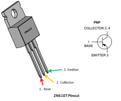
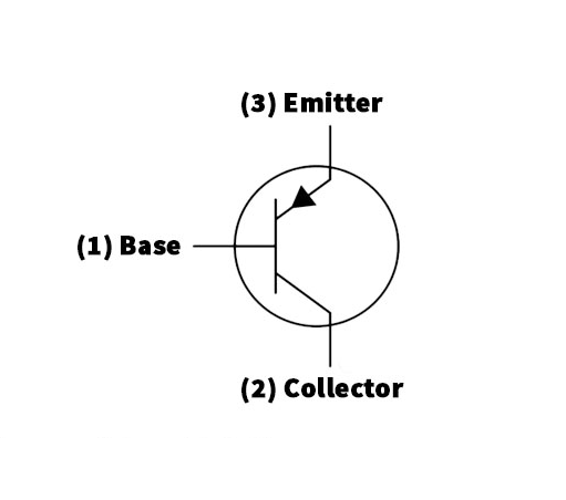
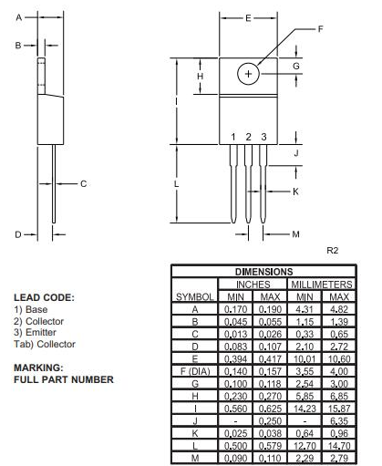
2N6107 Pin Configuration
|
Pin No. |
Pin Name |
Description |
|
1 |
Base |
Controls the biasing of the transistor, used to turn ON
or OFF the transistor |
|
2 |
Collector |
Current flows in through the collector, normally
connected to the load |
|
3 |
Emitter |
Current drains out through the emitter, normally
connected to ground |
Discovering the 2N6107 CAD Model
Symbol Representation
Circuit Footprint

Three-Dimensional Visualization
Key Attributes of the 2N6107 Transistor
The 2N6107 is a noteworthy PNP transistor, appreciated for its amplification prowess, with a gain spanning 30 to 150. This variability fits applications that seek moderate to strong amplification, creating pathways for its integration into diverse circuits. While supporting a maximum of 7A through the collector, it reflects limitations in high-current scenarios, inviting contemplation of alternative components for such demands. Under proper biasing, it consistently accommodates 7A between the collector and emitter.
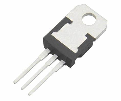
Its Base Emitter ON Voltage (VBE ON) reaches up to 3V when IC is 7A and VCE is 4V. This setting becomes useful when designing circuits focused on switching efficiency alongside power amplification. Enclosed in a TO220 package, the metal tab ingrained serves a dual function. It ensures a dependable electrical connection for the collector and aids in thermal management. This exact design becomes favorable for high-power deployments, where adept heat dissipation fosters stability and extends longevity in challenging environments.
The transistor's attributes render it well-suited for power amplification and switching tasks. Handling up to 7A while maintaining consistent performance parallels strategies in electrical production that blend efficient thermal management with electrical functionality. Employing the 2N6107 demands a thoughtful examination of thermal conditions, ensuring operations remain within defined parameters to stave off performance setbacks. This mirrors esteemed practices in circuit design, where precision and adherence to specifications are dominant to productive outcomes.
Functionality of the 2N6107 PNP Transistor
The 2N6107 PNP transistor becomes active without base current and deactivates when the current is present. In practical terms, it conducts when the base voltage is lower than the emitter voltage, owing to the n-type semiconductor base and p-type emitter. Exploring the nature of these materials reveals distinctions in how readily current flows or is obstructed.
The intricate relationship between base and emitter voltages plays an active role. You can appreciate the subtle balance required to maintain efficient current flow, reflecting a blend of scientific insight and practical intuition. When integrating the 2N6107 into circuits, adjusting the biasing is basic to achieving the desired operation.
• In amplification circuits, precise voltage alignment is useful to maintain performance. Even slight changes in voltage levels can notably affect the device's function, a lesson learned through hands-on experience. Circuit simulations commonly foresee and fix potential issues before physical implementation.
• Advanced configurations allow the 2N6107 to be used in switch-mode power supplies or audio amplification. Attention to thermal management is used to extending the transistor's life, as understanding its behavior can lead to creative circuit solutions.
Feature of 2N6107
|
Feature |
Specification |
|
Collector-Emitter Voltage (Vce) |
-70 V |
|
Collector-Base Voltage (Vcb) |
-80 V |
|
Emitter-Base Voltage (Veb) |
-5 V |
|
Collector Current (Ic) |
-7 A |
|
Collector Dissipation (Pc) |
40 W |
|
DC Current Gain (hfe) |
30 to 150 |
|
Transition Frequency (ft) |
4 MHz |
|
Operating and Storage Junction Temperature Range |
-65 to +150 °C |
|
Package |
TO-220 |
Applications of 2N6107
Circuit Design
For the effective deployment of the 2N6107 transistor, ensure the emitter voltage is higher than the base voltage. Connect the emitter to the positive terminal of a power source, like a 9V DC battery, while the negative connects to the base. Incorporating a diode at the emitter or ground terminal facilitates activation when the base voltage drops below the emitter's level.
Handling High Power
The 2N6107 is adept at managing substantial power, offering efficiency in driving high current loads. It proves to be a superior choice for larger load management, with applications emphasizing its performance where strong current handling is advantageous.
Effective Load Distribution
In scenarios of high demand, skillful power management becomes a must. The 2N6107 offers an opportunity to sustain efficient load distribution. Thoughtful placement in circuit design can diminish unwanted power waste, catering to those skilled in optimizing electronic componentry.
Module Drivers
The adaptability of the 2N6107 transistor makes it well-suited for tasks involving module drive, including relays and LED drivers. Its durability facilitates stable performance in switching operations, offering efficient control across a range of electronic scenarios. Harnessing its high current gain often satisfies you by enhancing both circuit efficiency and lifespan.
Audio and Signal Amplification
For audio and signal boosting, the 2N6107 excels in low-frequency amplification, intriguing audiophiles, with its ability to deliver clear sound and preserve signal quality. This extends to musical equipment, where it plays a role in producing superior sound experiences.
Darlington Pair Configurations
In the world of electronic design, the 2N6107 is often configured in Darlington pairs for increased current output. This arrangement significantly boosts current gain, easing the control of high-power devices with minimal input current. Such configurations are prevalent in power control applications, allowing smooth transitions and effective energy management. Successfully implementing these transistors involves a subtle grasp and exacting engineering to ensure peak performance.
Alternative Transistors for 2N6107
• NTE197 (PNP)
• 2N6110 (PNP)
Complementary NPN Transistor of 2N6107
• 2N6292
2N6107 Packaging
Manufacturer Info for 2N6107
Founded in 1974, Central Semiconductor has been at the forefront of crafting discrete semiconductor solutions for a myriad of electronic applications worldwide. Their extensive range includes small-signal transistors. bipolar power transistors, MOSFETs, and various diodes. With precise execution and innovative strides, they successfully meet the exact demands of technology.
Central's offerings extend beyond the ordinary with both industry-standard surface mount and through-hole devices. Their specialty lies in custom configurations such as bare die, TLMs (Thin Leadless Molded packages), and MDMs (Multi-Die Modules). These tailored solutions bring enhanced performance tailored to specific needs, revealing a finer understanding of individual requirements.
Central Semiconductor is acclaimed for its precise product quality and timely delivery. This dedication has resonated with global manufacturers, ensuring a dependable supply chain and exemplary service, driven by a shared trust in component consistency and precision. Their expertise in crafting semiconductors to exact standards allows Central to tackle technical challenges effectively.
Specifications of 2N6107
|
Type |
Parameter |
|
Factory Lead Time |
12 Weeks |
|
Mount |
Through Hole |
|
Package / Case |
TO-220 |
|
Collector-Emitter Breakdown Voltage |
70V |
|
Number of Elements |
1 |
|
Power Dissipation (Max) |
40W |
|
hFE Min |
30 |
|
Published |
2001 |
|
JESD-609 Code |
e0 |
|
Pbfree Code |
No |
|
Part Status |
Active |
|
Number of Terminations |
3 |
|
ECCN Code |
EAR99 |
|
Terminal Finish |
Tin/Lead (Sn/Pb) |
|
Max Operating Temperature |
150°C |
|
Min Operating Temperature |
-65°C |
|
HTS Code |
8541.29.00.95 |
|
Peak Reflow Temperature (°C) |
Not Specified |
|
Time@Peak Reflow Temperature-Max (s) |
Not Specified |
|
Pin Count |
3 |
|
JESD-30 Code |
R-PSFM-T3 |
|
Qualification Status |
Not Qualified |
|
Polarity |
PNP |
|
Element Configuration |
Single |
|
Case Connection |
COLLECTOR |
|
Transistor Application |
SWITCHING |
|
Gain Bandwidth Product |
10MHz |
|
Collector Emitter Voltage (VCEO) |
3.5V |
|
Max Collector Current |
7A |
|
Transition Frequency |
4MHz |
|
Frequency - Transition |
4MHz |
|
Collector Base Voltage (VCBO) |
80V |
|
Emitter Base Voltage (VEBO) |
5V |
|
DC Current Gain-Min (hFE) |
30 |
|
Continuous Collector Current |
450mA |
|
RoHS Status |
RoHS Compliant |
|
Lead Free |
Lead Free |
Frequently Asked Questions [FAQ]
1. What is the gain value of 2N6107?
The gain value of the 2N6107 transistor typically varies from 30 to 150, reflecting its versatility across diverse circuit designs. By grasping this range, you can choose suitable components, encouraging creativity and precision in achieving specific performance objectives. This adaptability empowers you to optimize circuits effectively, enhancing their sense of accomplishment.
2. What is the packaging type of 2N6107?
The 2N6107 utilizes TO220 compact packaging, admired for its heat dissipation efficiency and simplicity in installation. Its sturdy characteristic suits environments constrained by space while emphasizing thermal performance. Experts often select this packaging for its adept balance of size and functionality in intricate circuit configurations, appreciating its contribution to streamlined design efforts.
3. What applications favor the use of 2N6107?
The 2N6107 excels in power amplification and switching functions, tailored for situations demanding consistent power management and swift switching capabilities. It finds its place in practical applications like audio systems and power supplies, where its efficiency and cost advantages coexist harmoniously. This synergy is treasured in sectors that value both power management and budget considerations, resonating well with those who navigate the delicate dance between performance and practicality.