A Comprehensive Guide to SN74LVC1G17QDCKRQ1 Schmitt-Trigger Buffer
The SN74LVC1G17QDCKRQ1, is a robust Schmitt-trigger buffer that supports a broad voltage range of 1.65 to 5.5 V VCC, making it adaptable to various electronic applications. This article explores its design, pin configuration, datasheet highlights, and key features, providing you with the insights needed for reliable integration. With strong noise immunity and precise threshold levels, this component is ideal for stabilizing digital circuits, even in challenging environments. Dive in to discover how the SN74LVC1G17QDCKRQ1 enhances performance in diverse projects and delivers effective signal conditioning and level translation.Catalog
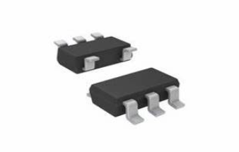
Overview of SN74LVC1G17QDCKRQ1
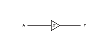
The SN74LVC1G17QDCKRQ1 serves as a Schmitt-trigger buffer, adeptly implementing the Y = A Boolean function. Its design embraces a broad voltage spectrum, providing flexibility for a variety of uses. Leveraging CMOS technology, it delivers elevated output levels while curbing static power usage. Multiple packaging options further contribute to its suitability for various circuit configurations.
The expansive voltage range of the SN74LVC1G17QDCKRQ1 responds to diverse supply voltage needs found in contemporary digital systems. This adaptability ensures harmonious operation and reliability across multiple platforms. Its energy-efficient nature aligns with modern calls for technology that respects resource conservation.
Deployment of the buffer in practical scenarios highlights the reduction of static power consumption as instrumental in fostering energy-efficient functionality. You can frequently select such components for battery-operated devices where extending battery duration takes precedence. This experience emphasizes the role of CMOS technology in refining performance without excessive energy use.
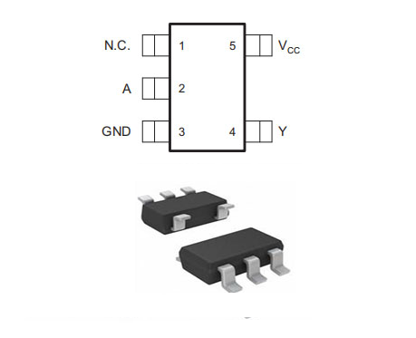
Pin Configuration
|
Pin Number |
Pin Name |
Description |
|
1 |
NC |
Not connected |
|
2 |
A |
Input |
|
3 |
GND |
Ground |
|
4 |
Y |
Output |
|
5 |
VCC |
Power terminal |
CAD Design
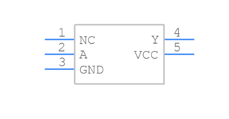
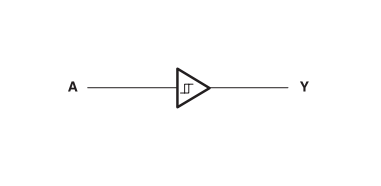
Symbol Representation
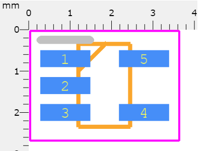
Circuit Board Footprint
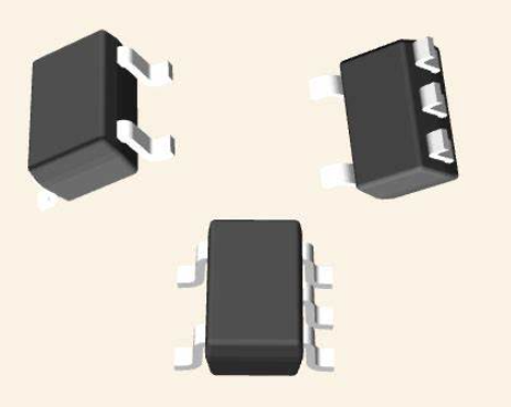
3D Visualization
Features
|
Feature |
Description |
|
Qualified for Automotive Applications |
Yes |
|
Supports 5-V VCC Operation |
Yes |
|
Input Voltage Range |
Accepts voltages up to 5.5 V |
|
Maximum Propagation Delay (tpd) |
8 ns at 3.3 V |
|
Power Consumption |
Low, with a maximum ICC of 20 μA |
|
Output Drive Capability |
±24 mA at 3.3 V |
|
Ioff Support |
Supports live insertion, partial-power-down mode, and
back-drive protection |
|
ESD Protection |
JEDEC JS-001 compliant |
|
Human-body Model ESD Protection |
2000 V |
|
Charged-device Model ESD Protection |
1000 V |
Technical Specifications
|
Type |
Parameter |
|
Lifecycle Status |
ACTIVE (Last Updated: 4 days ago) |
|
Factory Lead Time |
6 Weeks |
|
Mount |
Surface Mount |
|
Mounting Type |
Surface Mount |
|
Package / Case |
5-TSSOP, SC-70-5, SOT-353 |
|
Number of Pins |
5 |
|
Operating Temperature |
-40°C ~ 125°C TA |
|
Packaging |
Tape & Reel (TR) |
|
Series |
Automotive, AEC-Q100, 74LVC |
|
JESD-609 Code |
e4 |
|
Pbfree Code |
Yes |
|
Part Status |
Active |
|
Moisture Sensitivity Level (MSL) |
1 (Unlimited) |
|
Number of Terminations |
5 |
|
ECCN Code |
EAR99 |
|
Terminal Finish |
Nickel/Palladium/Gold (Ni/Pd/Au) |
|
Packing Method |
TR |
|
Voltage - Supply |
1.65V ~ 5.5V |
|
Terminal Position |
DUAL |
|
Terminal Form |
GULL WING |
|
Peak Reflow Temperature (Cel) |
260 |
|
Number of Functions |
1 |
|
Supply Voltage |
1.8V |
|
Frequency |
100MHz |
|
Base Part Number |
74LVC1G17 |
|
Pin Count |
5 |
|
Output Type |
Push-Pull |
|
Polarity |
Non-Inverting |
|
Power Supplies |
3.3V |
|
Number of Channels |
1 |
|
Nominal Supply Current |
500nA |
|
Propagation Delay |
6 ns |
|
Quiescent Current |
20μA |
|
Input Type |
Schmitt Trigger |
|
Turn On Delay Time |
14 ns |
|
Family |
LVC/LCX/Z |
|
Logic Function |
Buffer, Schmitt Trigger |
|
Output Characteristics |
3-STATE |
|
Logic Type |
Buffer, Non-Inverting |
|
Max I(ol) |
0.032 A |
|
Schmitt Trigger |
YES |
|
Power Supply Current-Max (ICC) |
0.02mA |
|
Number of Output Lines |
1 |
|
Ambient Temperature Range High |
125°C |
|
Height |
1.1mm |
|
Length |
2mm |
|
Width |
1.25mm |
|
Thickness |
900μm |
|
REACH SVHC |
No SVHC |
|
Radiation Hardening |
No |
|
RoHS Status |
ROHS3 Compliant |
|
Lead Free |
Lead Free |
Comparable Components
|
Part Number |
Manufacturer |
Package / Case |
Number of Pins |
Logic Function |
Propagation Delay |
Supply Voltage |
Technology |
Mount |
Terminal Position |
View Compare |
|
SN74LVC1G17QDCKRQ1 |
Texas Instruments |
5-TSSOP, SC-70-5, SOT-353 |
5 |
Buffer, Schmitt Trigger |
6 ns |
1.8 V |
CMOS |
Surface Mount |
DUAL |
SN74LVC1G17QDCKRQ1 |
|
SN74LVC2G04DCKR |
Texas Instruments |
6-TSSOP, SC-88, SOT-363 |
6 |
- |
8 ns |
1.8 V |
CMOS |
Surface Mount |
DUAL |
SN74LVC1G17QDCKRQ1 VS SN74LVC2G04DCKR |
|
SN74AHCT1G14DCKR |
Texas Instruments |
5-TSSOP, SC-70-5, SOT-353 |
5 |
Buffer, Inverter |
7.5 ns |
3.3 V |
CMOS |
Surface Mount |
DUAL |
SN74LVC1G17QDCKRQ1 VS SN74AHCT1G14DCKR |
|
SN74AHC1G04DCKRE4 |
Texas Instruments |
5-TSSOP, SC-70-5, SOT-353 |
5 |
Buffer, Inverter |
7.5 ns |
3.3 V |
CMOS |
Surface Mount |
DUAL |
SN74LVC1G17QDCKRQ1 VS SN74AHC1G04DCKRE4 |
|
MC74VHC1G05DFT2 |
ON Semiconductor |
5-TSSOP, SC-70-5, SOT-353 |
5 |
Buffer, Inverter, Schmitt Trigger |
8 ns |
5 V |
CMOS |
Surface Mount |
DUAL |
SN74LVC1G17QDCKRQ1 VS MC74VHC1G05DFT2 |
Functional Diagram
Simplified Schematic
Typical Use
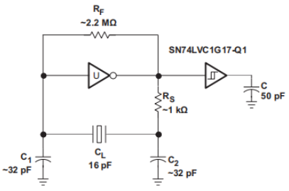
The SN74LVC1G17QDCKRQ1 device is distinguished by its balanced output drive, thanks to its CMOS structure. Elevating its performance involves addressing bus congestion, which could lead to excessive current flow and possible component damage. Quick signal transitions into light loads require careful routing to prevent issues such as signal ringing.
Design Guidelines
Inputs should remain stable in multi-bit logic devices. Floating inputs occur when, for example, only two inputs of a triple-input AND gate are utilized, or when three out of four buffer gates are in use. With many functions or parts left idle, external connections may carry undefined voltages, leading to unpredictable operating states. Such input terminals should stay connected.
To address floating, connect all unused inputs of digital logic devices to either a high or low bias. The specific logic level applied to unused inputs is guided by the device’s intended function. Typically, connecting unused inputs to GND or Vcc is common, and chosen based on necessity or convenience.

Alternatives
|
Part Number |
Description |
Manufacturer |
|
SN74LVC1G17DCKTE4LOGIC |
Single 1.65-V to 5.5-V buffer with Schmitt-Trigger
inputs, 5-SC70, -40 to 125°C |
Texas Instruments |
|
74LVC1G17GWLOGIC |
IC LVC/LCX/Z Series, 1-Input Non-Invert Gate, PDSO5,
Plastic, MOC-203, SC-88A, SOT353-1, TSSOP-5, Gate |
NXP Semiconductors |
|
74LVC1G17GW-Q100 |
Buffer, LVC/LCX/Z Series, 1-Function, 1-Input, CMOS,
PDSO5 |
Nexperia |
Potential Applications
AV Receivers
AV receivers serve as the center of home entertainment, merging sound and visuals for an engaging experience. Modern versions not only elevate audio quality but also support streaming and smart home connectivity. As preferences shift, these systems might embrace voice commands and AI-driven content, paving the way for more intuitive interactions.
Portable Audio Docks
Portable audio docks provide both convenience and rich sound. Innovations often aim to boost battery longevity and fidelity. With advances in Bluetooth technology, connectivity has seen notable improvements. They are ideal for outdoor events and gatherings, offering a seamless mix of flexibility and robust sound.
Blu-Ray and Home Theaters
Blu-ray players and home theaters, popular for high-definition content, now feature 4K support and advanced audio like Dolby Atmos. As digital streaming rises, hybrid models blending physical media and streaming services are emerging, providing diverse viewing experiences while still valuing physical media collections.
MP3 Devices
Amid the streaming era, MP3 devices still appeal due to their portability and offline use. Enhancements in storage and sound attract users who enjoy customizing music libraries. Insistent in areas with limited internet, they guarantee continuous listening enjoyment.
PDAs
Traditional PDAs influence today's smartphones and tablets, integrating personal management, connectivity, and multimedia functionality. Future models may leverage AI and machine learning for predictive tasks and tailor your experiences, enriching productivity on the go.
Telecom Power Supplies
Supporting data centers and networks, telecom power supplies focus on being efficient and reliable. With data demands escalating, innovations in energy storage and conversion help reduce power loss. Reliable service is especially vital in regions with power issues, stabilizing telecommunication operations.
SSDs
SSDs have transformed data storage, offering speed and resilience. As research pushes for larger, budget-friendly options, SSDs continue to replace traditional drives. This is evident in enterprise centers prioritizing rapid data access, influencing cloud services and personal computing alike.
HDTVs and Digital TVs
HDTVs and digital TVs mark a major step in clarity and technology. Now equipped with smart features, they integrate streaming and voice assistants. Advancements like OLED and QLED enhance vividness, elevating home viewing experiences significantly.
Enterprise Tablets
Designed for business flexibility, enterprise tablets offer power and portability. Security and enterprise applications ensure data safety. In fields like healthcare and logistics, they optimize workflows, showing the shifting trend toward mobile solutions.
Video Analytics Servers
In sectors like security and research, video analytics servers are key. Utilizing AI, they improve video analysis, enabling insights. An example is in smart city design, aiding traffic control and public safety, highlighting tech's role in urban development.
Wireless Peripherals
Wireless peripherals such as keyboards and mice offer a tidy, flexible workspace. Enhanced Bluetooth protocols improve interaction across devices. These peripherals adapt to corporate and personal settings alike, focusing on your ease and comfort.
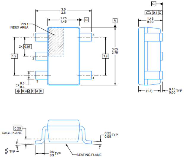
Package
Manufacturer Insights
Texas Instruments (TI) plays a major role in the semiconductor industry, continuously exploring new technological frontiers. Their specialized skills in crafting and promoting analog and embedded processing chips keep them at the helm of innovation. TI operates in 35 countries, reflecting a dedication to offering advanced solutions across various markets. This expansive global presence fosters a vibrant exchange of ideas and technologies, allowing them to meet diverse consumer expectations with precision.
The TI workforce is deeply involved in nurturing a culture that thrives on creativity and strategic foresight. This environment not only sparks innovative thinking but also propels the development of solutions that align with evolving technological landscapes. Backgrounds provide invaluable insights, enhancing the company’s innovative prowess. TI's advancements in analog and embedded processing profoundly affect sectors such as automotive, industrial, and consumer electronics. These innovations enhance existing technologies and create new potential applications, setting new standards within the industry.
Datasheet PDF
SN74LVC2G04DCKR Datasheets:
SN74AHCT1G14DCKR Datasheets:
MC74VHC1G05DFT2 Datasheets:
Cylindrical Battery Holders.pdf
Frequently Asked Questions [FAQ]
1. What Is the Operating Voltage Range?
The operational voltage range covers 1.65 to 5.5 V VCC. This adaptable range accommodates diverse applications across various devices, allowing integration into multiple electronic systems. In practical scenarios, maintaining this range can enhance both stability and efficiency, aligning with the complex requirements of intricate circuitry. This adaptability often appeals to engineers who seek to balance efficiency with diverse operational demands.
2. How Does the Boolean Function Perform?
This device performs the Y = A function, indicating a direct correlation where the output replicates the input. Its straightforwardness aids usage in digital circuits where uncomplicated logic processing is desired. You can often appreciate this simplicity as it minimizes complexity, fostering reliability and predictability within systems. This direct approach aligns well with those valuing clear and efficient circuit design.
3. What Is the Advantage Of a Wide VCC Range?
It features high output drive capabilities, supporting robust functionality under varying voltage conditions. This broadens the scope of potential applications as you can tailor circuitry to handle different load conditions, promoting consistent performance even in dynamic environments. This characteristic frequently becomes a focal point for those looking to maximize device efficacy across variable contexts.
4. What Package Options Are Available?
A variety of packages are available, addressing diverse design and spatial requirements. This selection equips engineers with the flexibility to determine the best package for specific needs, whether compact or expansive. Adaptable packaging ensures adherence to industry standards, fostering efficient implementation in various operational settings. This versatility often proves invaluable to you seeking harmony between form and function.